
Carbon Nanotubes
Carbon Nanotubes (CNTs) are of profound interest in a myriad of fields of research and industry. These allotropes of carbon are exteremely strong and exhibit unqiue thermal conductive, mechanical, and electrical qualtiies.
AFM together with Raman based methods have become the method of choice for characterizing carbonaceous materials. AFM-Raman imaging is especially useful for differentiating the different kinds of nanotubes. Nanonics Multiprobe SPM Systems enable thermal, electrical, and optical transport studies on carbon naotubes. Photoconductivity , Raman and TERS, as well as SNOM/NSOM measurements, are all available in a variety of environments within the same platform.
Results
1. AFM Raman

AFM image of carbonaceous material on silicon

Raman spectra map of carbonaceous material on silicon

Raman intensity map of carbonaceous material on silicon
(Left) - A 10um x 10um AFM topography image of carbonaceous material on silicon clearly showing the presence of a nanotube on the surface in addition to some round carbonaceous domains at the top and bottom two corners.
(Center) - Raman spectra were collected both on the nanotube and the circular domains. Below the red spectrum corresponds to the Raman spectrum on the nanotube showing a large peak at 1575cm-1 and a smaller peak at about 1340cm-1. A Raman spectrum from the round domains is shown in green revealing a large peak at 1340cm-1 and a weak, dual peak at about 1600cm-1. These spectra clearly differentiate the carbon nanotube and the surrounding disordered material.
(Right) - A Raman intensity map at 1600cm-1 and 1340cm-1 was collected with the resulting image shown below, clearly mapping the carbon nanotube (red) and the regions of disordered materials (Green).
2. TERS

AFM Image of a cluster of carbon nanotubes

TERS map with the probe in contact with the sample showing the Raman intensity at 405cm-1.

TERS map with the probe retracted again showing the Raman intensity at 405cm-1.

TERS difference map (comparing the two maps to the left)
A TERS probe was used to collect Raman difference spectra of carbon nanotube clusters in the images shown above.
(Top) - An AFM topography map of the clusters is shown above, revealing several hundred nanometer round domains of carbon nanotubes.
(Left) - A TERS map with the probe in contact with the sample was collected, showing the Raman intensity at 405cm-1. The Raman map was collected at an array of 1850 points (pixels shown in the topography image) where measurements were separated by 180nm.
(Center) - The tip is then retracted, and the far-field Raman intensity map at 405cm-1 is again collected.
(Right) - The difference map between the first two maps is shown, clearly providing significantly better resolution in the Raman intensity map that can be accurately correlated with the intial AFM topographic map, revealing important chemical information about the various CNT clusters.
3. Conductive AFM Raman

AFM image of SW carbon nanotube
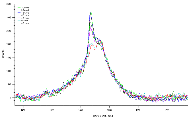
Map of Raman scattering G band of conducting SW CNTs
The Raman spectra show repeatably from 0 to 3V the large scattering at the G- band ~1570 cm-1 which defines the metallic character of many of the tubes in this bundle.
However, when the voltage is raised to ~5V and above the band decreases with voltage.
Nonetheless the g+ band which is independent of cnt diameter or chirality remains rigidly constant at these voltages, indicating that the reduction of g- band is not associated with cnt destruction but simply related to alteration by the high voltage of cnt character from conducting to non-conducting.
Publications
| A controllable way to measure the interfacial strength between carbon nanotube and polymer using a nanobridge structure |
| Nie, Min, Dilhan M. Kalyon, Kishore Pochiraju, and Frank T. Fisher. |
| Carbon 116 (2017): 510-517. |
| Application of a hole transporting organic interlayer in graphene oxide/single walled carbon nanotube–silicon heterojunction solar cells. |
| Yu, LePing, Munkhbayar Batmunkh, Tom Grace, Mahnaz Dadkhah, Cameron Shearer, and Joseph Shapter. |
| Journal of Materials Chemistry A 5, no. 18 (2017): 8624-8634. |
| Preparation of Surface Modified Multi-Walled Carbon Nanotubes Based Thin-Film Gas Sensor. |
| Mathew, E., V. Persis Preethi, and S. Rajesh. |
| Journal of Advanced Microscopy Research11, no. 2 (2016): 130-136. |
| Nanodrawing of Aligned Single Carbon Nanotubes with a Nanopen |
| Yeshua, Talia, Christian Lehmann, Uwe Hübner, Suzanna Azoubel, Shlomo Magdassi, Eleanor EB Campbell, Stephanie Reich, and Aaron Lewis. |
| Nano letters 16, no. 3 (2016): 1517-1522. |


