
Atomic Force Microscopy (AFM) provides a variety of nanometric characterizations such as topography, conductivity, and thermal measurements. While very effective at measuring certain properties, AFM can not identify the chemical composition of a given material. Raman spectroscopy, however, has emerged as a critical technique in the field of chemical characterization, accurately identifying and classifying materials in a number of diverse fields and industries such as: material science, chemistry, biophysics, semiconductors, and many more.
Harnessing the power of these two techniques enables a synergistic and holistic analysis of a given material. As early as 2001, Nanonics Imaging exhibited the foresight to combine the advantages of AFM and Raman by providing an integrated platform. The joint AFM-Raman system allows for the strength and versatility of all modes of AFM (including mechanical, thermal, SECM, and electrical) combined with the chemical characterization of Raman. Nearly two decades later, Nanonics Imaging continues to be at the vanguard of integrated optical AFM-Raman systems, providing solutions in the most challenging areas of research and in the most innovative fields in applied sciences: graphene and 2D materials, carbon nanotubes, semiconductor metrology, and molecular biology.

Key Features
Full Optical Integration
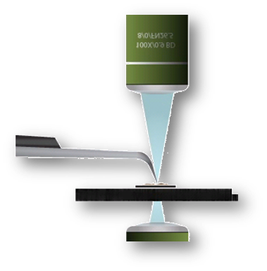
- Cantilevered glass AFM & TERS probes - exclusive for Nanonics systems
- Above and side views
- Compatibility with all third party probes

- High N/A with 1 mm working distance
TERS on All Samples
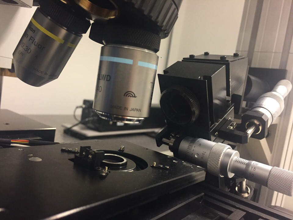
The simultaneous and independent SPM probe operation of up to 4 probes enables full characterization of all dimensions of samples and devices. All forms of SPM are enabled for each individual probe accompanied by total optical integration resulting in access to all modes including AFM, KPM, EFM, ANSOM, NSOM, STM, AFM-Raman, and TERS. Because these probes are designed for multiple probe operation, they can be brought to a nanometric separation distance thus ensuring that the same area is scanned with all the probes.
Advanced SPM with Correlated Raman
- Mechanical SPM
- Electrical SPM
- Thermal SPM
- Kelvin Probe SPM
Autofocus Raman Illumination
Autofocus ensures the same Raman illumination at every point, removing out-of-focus noise.
Seen below: 2 maps of diamond 1334 cm-1 intensity: first without and then with autofocus. Blue represents weaker Raman air signal due to varying focus.

Without autofocus.

With autofocus
AFM-Raman Applications
AFM Raman: Graphene

Single Layer (2676 cm-1 Map)

Double Layer (2700 cm-1 Map)

3D Collage of AFM Raman
Single Layer (2676 cm-1 Map)

3D Collage of AFM Raman
Double Layer (2700 cm-1 Map)
AFM-Raman - Conductive Single Walled Carbon Nanotubes
Raman demonstrates G- band of conducting CNT as a function of CAFM voltage. Significant loss of conductivity after 4V due to defect introduction from voltage.

CAFM Carbon Nanotubes

Correlated Raman Map

Nanonics NanoFountainpen Depositing CNTs
Deposited carbon nanotube(CNT) between two metallic contacts with Nanonics NanoFountainpen.
AFM-Raman - Biology

AFM Topography

Correlated Raman scattering at 1600 cm-1 with AFM topography
TERS Applications
TERS - Graphene
TERS: On-line AFM & STM with the Same Probe
Tuning forks allow for controlled contact AFM to reversibly at will generate defects in graphene with force


Featured Paper: “Reversible defect in graphene investigated by Tip-enhanced Raman spectroscopy. ”
Authors: Wang, P., Zhang, D., Li, L., Li, Z., Zhang, L., & Fang, Y.
Reference: Plasmonics, 7(3), 555-561. (2012)
TERS - On a Wide Variety of Substrates
Copper Phthalocyanine (CuPc) On Three Surfaces
TERS with a probe that allows for any surface has permitted TERS of CuPc molecules on a wide variety of substrates, including (as seen here) an interesting comparison of MoS2, Gold, and SiO2 surfaces.


Featured Paper: “Tip-Enhanced Raman Scattering on Bulk MoS2 Substrate”
Authors: He, Z., Voronine, D. V., Sinyukov, A. M., Liege, Z. N., Birmingham, B., Sokolov, A. V., ... & Scully, M. O.
Reference: IEEE Journal of Selected Topics in Quantum Electronics, 23(2), 113-118. (2017)
TERS - Biology
Human Colon Cancer Cells (SW480) - Differentiating Rgd-Integrin Binding on 4nm Membrane

Ligand-receptor interactions play important roles in many biological processes. Cyclic arginine – glycine – aspartic acid (RGD) containing peptides are known to mimic the binding domain of extracellular matrix protein fibronectin and selectively bind to a sub- set of integrin receptors on cell surfaces.

TERS of RGD-functionalized nanoparticles bound to integrin receptors produce Raman scattering signal specific to the bound receptor protein thus differentiating α5β1 and αvβ3 integrin receptors on cancer cell membranes.
Featured Paper: “Selective detection of RGD-integrin binding in cancer cells using tip enhanced Raman scattering microscopy.”
Authors: Xiao, L., Wang, H., & Schultz, Z. D.
Reference: Analytical chemistry, 88(12), 6547-6553. (2016)
Videos
Contact a Nanonics Specialist to Discuss Your Specific Needs
We are happy to answer all questions and inquiries
Configurations
Which Nanonics system configuration is right for your AFM-Raman research?
Publications
Read exemplary, peer-reviewed literature on studies using Nanonics AFM-Raman systems
| Local hole doping concentration modulation on graphene probed by tip-enhanced Raman spectroscopy |
| Iwasaki, T., Zelai, T., Ye, S., Tsuchiya, Y., Chong, H. M., & Mizuta, H |
| Carbon 111 (2017): 67-73. |
| Quantifying Defect Densities in Monolayer Graphene Using Near-field Coherence Measurements. |
| Naraghi, R. R., Cançado, L. G., Salazar-Bloise, F., & Dogariu, A. |
| Frontiers in Optics, pp. FF5B-3. Optical Society of America, 2016. |
| Organometallic-Constructed Tip-Based Dual Chemical Sensing by Tip-Enhanced Raman Spectroscopy for Diabetes Detection. |
| Lin, D., Lin, Y., Yang, S., Zhou, L., Leong, W. K., Feng, S., & Kong, K. V. |
| ACS applied materials & interfaces. (2018) |
| Enhanced graphene photodetector with fractal metasurface |
| Fang, Jieran, Di Wang, Clayton T. DeVault, Ting-Fung Chung, Yong P. Chen, Alexandra Boltasseva, Vladimir M. Shalaev, and Alexander V. Kildishev. |
| Nano letters 17, no. 1 (2016): 57-62. |