
AFM
The Advantages of Nanonics VISTA
Atomic Force Microscopy (AFM) provides a variety of nanometric characterizations such as topography, conductivity, and thermal measurements. Nanonics offers unique AFM technology - VISTA (Vivid Imaging Soft Touch AFM). This innovation offers ultrasensitive single pN force mapping combined with the benefits of super-resolution optical/fluorescent imaging. See below for some of the key features and cutting edge applications of VISTA.
What Nanonics Customers have Published:
…high sensitivity in amplitude and phase, as well as high mechanical quality factor…. it provides conclusive information about the morphology of one-dimensional nanostructures.”
Key Features
Click on any feature to learn more
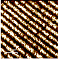
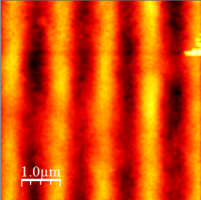
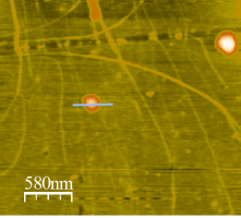
Superior AFM Imaging
Obtain highest resolution imaging with VISTA.
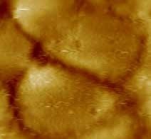
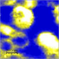
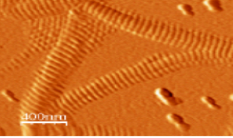
Topography of living MDCK cells imaged with Nanonics VISTA showing microvilli.
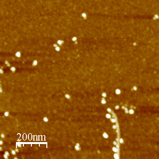
DNA decorated with quantum dots.
What customers publish: "…tuning fork configuration (intermittent mode) presents advantages over the beam bounce configuration (contact mode) namely high sensitivity in amplitude and phase, as well as high mechanical quality factor…. it provides conclusive information about the morphology of one-dimensional nanostructures."
Featured Paper: “Atomic force microscopy (AFM) and 3D confocal microscopy as alternative techniques for the morphological characterization of anodic TiO2 nanoporous layers.”
Authors: Oyarzún, D. P., Pérez, O. E. L., Teijelo, M. L., Zúñiga, C., Jeraldo, E., Geraldo, D. A., & Arratia-Perez, R.
Reference: Material Lett.165, 67–70 (2016)
No Jump to Contact
High stiffness with high sensitivity. No jump to contact AFM allows for true non-contact & switching on-line from AFM to tunneling feedback with the same probe.
Dual Feedback
No feedback laser noise for many functional measurements, including NSOM. Nanonics systems can employ standard beam bounce feedback silicon probes & ultrasensitive tuning fork feedback.
Highest Force Sensitivty
VISTA allows for the highest force sensitivity of any AFM: down to single pNs. This is effectively demonstrated in papers where force measurements down to <5 pNs are shown.
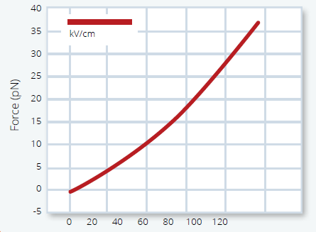
Study ofT Lymphocyte Jurkat cells - graph indicating the signficantly improved force sensitivity that can be achieved with Nanonics AFM technology, as compared to conventional AFMs.
Featured Paper: “Effects of nanosecond pulse electric fields on cellular elasticity”
Authors: Dutta, D., Asmar, A., & Stacey, M.
Reference: Micron, 72, 15-20. (2015)
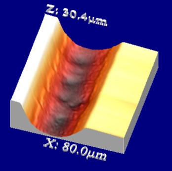
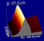
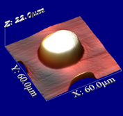
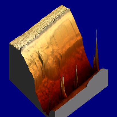
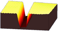
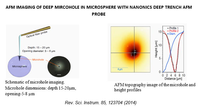
Large Z Range
Nanonics probes and scanners enable imaging of high aspect ratio deep trenches and protrusions not previously possible:
- Large Z scanning range: 85µ
- Long tip length of >100µ or greater
- Very high 10:1 aspect ratio glass probes
Cardiac stent
Razor blade tip
Contact Lens
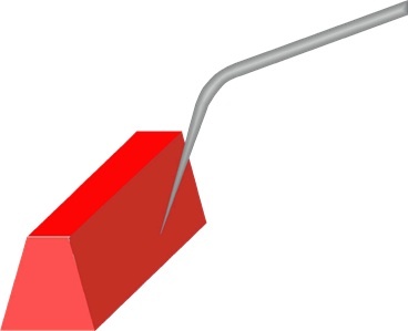
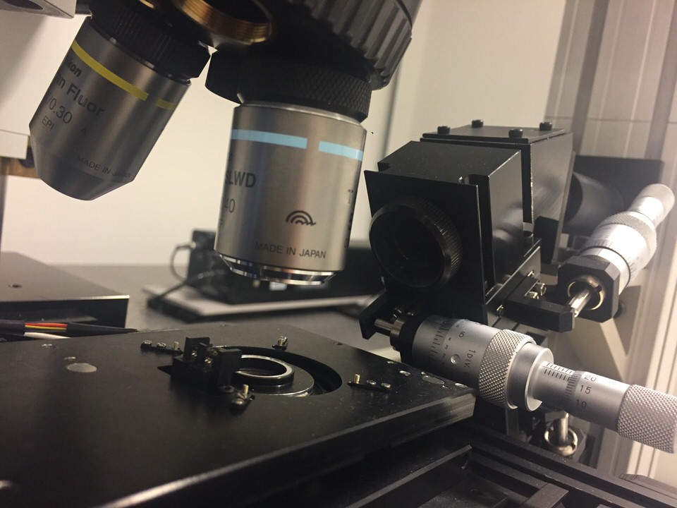
Unique Glass Probes
Applications
Side Wall Imaging
Unprecedented side wall imaging with the exposed tip of glass probes
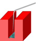
Deep Trench Imaging
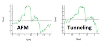
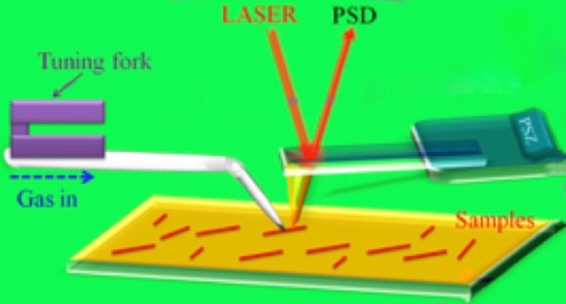
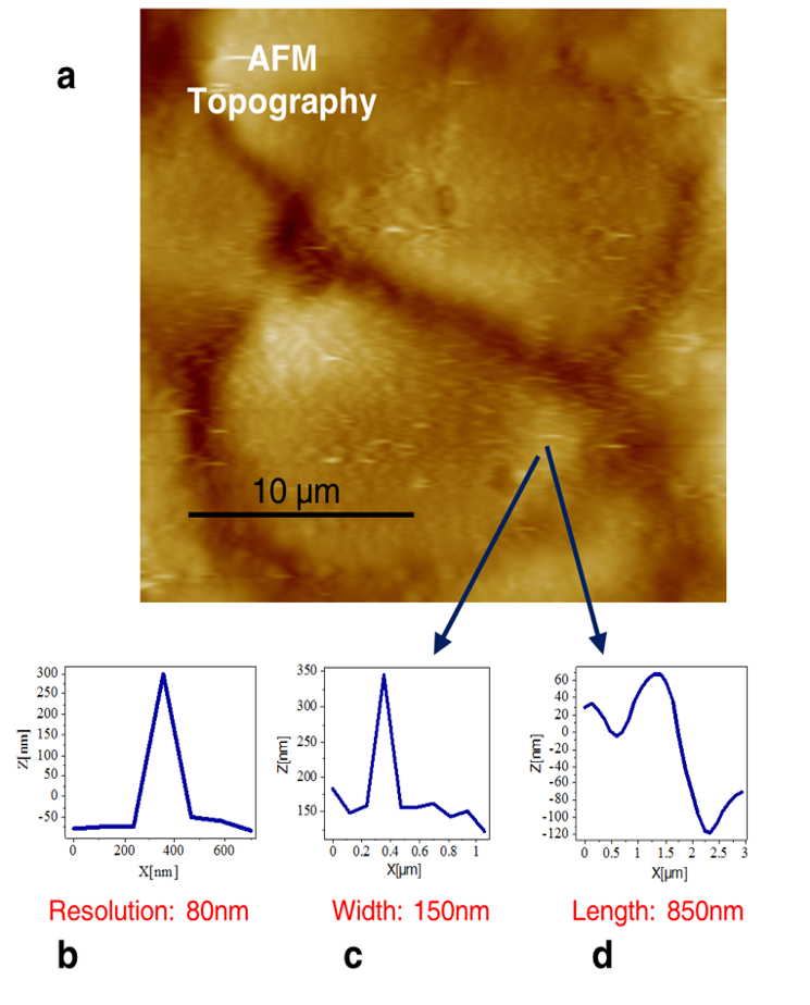
Elasticity of Microvilli in MDCK Cells
Microvilli in live MDCK cells with a cantilevered glass probe attached to tuning fork.
Q factor in liquid 5000 normally 4 or 5 with beam bounce methods silicon cantilevers.
Only in 2016 were very specialized silicon cantilevers able to image this structure and even these cantilevers could not approximate the ideal of glass probes and so were not able to measure the elasticity.
Images
Error

Videos
SEM Movie of AFM Probe Scanning a Grating
AFM Controlled Deposition & Imaging of Cells
Topographical & Thermal Measurements
Intro to AFM and Feedback Technology
Ease of Probe Mounting
Contact a Nanonics Specialist to Discuss Your Specific Needs
We are happy to answer all questions and inquiries
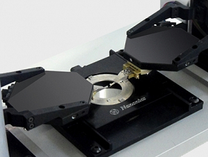
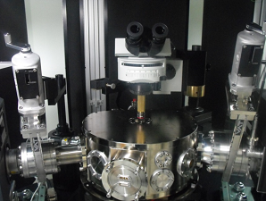
Configurations
Which Nanonics system configuration is right for your AFM research?
Publications
Read exemplary, peer-reviewed literature on studies using Nanonics AFM systems
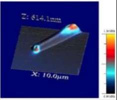
Best CAFM Results in Comparative Study
Unique Technology Avoids Photocurrent Artifacts
Review of Scientific Instruments 87(8), 083703
Yanfeng Ji, Fei Hui, Yuanyuan Shi, Vanessa Iglesias, David Lewis, Jiebin Niu, Shibing Long, Ming Liu, Alexander Hofer, Werner Frammelsberger, Guenther Benstetter, Andrew Scheuermann, Paul C. McIntyre and Mario Lanza
Photoactive materials play a crucial role in the development of energy storage devices, such as solar, electrochemical cells, and others. Conductive atomic force microscopy (CAFM) is a powerful tool for nanoscale electronic characterization of photoactive materials. It is well known that environmental light can alter the measurements when scanning photoactive samples. For this reason, measuring in a dark environment has been recognized as the standard CAFM process. However, as an optical feedback laser is necessary to acquire topography, the laser used in CAFM can also generate a high photocurrent, even without any bias between the conductive tip and the sample. While the laser-induced current signal perturbation is well known within the CAFM community, the observation of currents generated by the optical feedback laser in absence of bias is still not fully understood and has never been studied in depth.
For the first time, this paper studies and analyzes the photocurrent induced in the photoactive materials by the feedback laser. CAFM measurements were carried out on photoactive samples using six standard optical feedback AFMs of different manufacturers, as well as a Nanonics tuning-fork based feedback AFM (without using a laser).
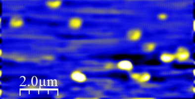
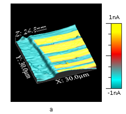
Seen in image: 3D Collage Map of topographic and current maps, collected on Ni electrode using the Nanonics MV4000 AFM without application of bias. The yellow regions were measured with illumination, in order to replicate a feedback laser, and high current is observed. In contrast, the blue regions were measured without any feedback laser, and thus in absolute darkness, and no current is observed.
| Atomic force microscopy (AFM) and 3D confocal microscopy as alternative techniques for the morphological characterization of anodic TiO2 nanoporous layers |
| Oyarzún, D. P., Pérez, O. E. L., Teijelo, M. L., Zúñiga, C., Jeraldo, E., Geraldo, D. A., & Arratia-Perez, R. |
| Materials Letters, 165, 67-70. |
| Reduction in Step Height Variation and Correcting Contrast Inversion in Dynamic AFM of WS 2 Monolayers |
| Godin, K., Cupo, C., & Yang, E. H. |
| Scientific reports, 7(1), 17798. |
| Live cell near-field optical imaging and voltage sensing with ultrasensitive force control |
| Brahami, A., Levy, H., Zlotkin-Rivkin, E., Melamed-Book, N., Tal, N., Lev, D., ... & Lewis, A. |
| Optics express, 25(11), 12131-12143. |
| Fast Current Blinking in Individual PbS and CdSe Quantum Dots. |
| Maturova, K., Nanayakkara, S. U., Luther, J. M., & van de Lagemaat, J. |
| Nano letters, 13(6), 2338-2345. |