AFM SEM/FIB
Scanning electron microscopy (SEM) and ion beam milling techniques are mature nanoscale measurement technologies, whereas atomic force microscopy (AFM) is a developing technology generating intense interest in the scientific community for basic research and development. These techniques have generally existed in separate worlds. This article discusses a capability that marries these technologies through an instrument recently introduced by Nanonics. Hybrid methodologies are becoming more important as research needs continue to push the development of characterization tools that provide a more complete understanding of materials. In combination with the growing and pervasive needs of nanotechnology, the use of hybrid methods to study material properties with nanoscale spatial resolution is at the forefront of instrumentation in both research laboratories and industry.
Development focused both on instrumental compatibility and on the new research directions that such a combined tool could take for improved characterization of materials. The development of the Nanonics 3TB4000 has been a part of an integrated microscopy program, which included combining light optics with AFM [1], Raman chemical analysis and AFM [2], and mass spectroscopy with AFM functionality [3]. These technique combinations have resulted in unique capabilities unachievable with any of the above instruments alone. This article gives the reader a first glimpse at the emerging union of AFM with SEM/FIB.

Figure 1: Schematic of an ultraflat scanner geometry design for confined spaces including electron and ion optical integration.
Quick Links
Innovative Design
The challenge has been, as in all such integrations, to maintain full functionality of each individual technique while at the same time enabling new materials characterization capabilities through integration that did not exist previously. Historically there have been several barriers to the effective merger of AFM methodologies with other microscopical or analytical techniques. This section describes the innovations in scanner, probe, and feedback loop technology and design to overcome these barriers.
Scanner
The AFM scanner controls the fine X, Y, and Z motion of either the sample or the tip in the instrument, depending on the instrument configuration. These scanners often employ cylindrical piezoelectric elements. These elements in the upright configuration possess limited Z range and a geometry that obstructs integration with an electron and ion beam. On the other hand, a cylindrical piezo device permits large ranges of X and Y motion perpendicular to the long axis of the piezo. To thisend Nanonics has developed a 3D UltraFlat Scanning stage with 4 cylindrical piezos (see schematic in Figure 1), enabling large ranges (85 µm or greater) in X, Y, and Z. This new stage allows for a variety of geometries of AFM systems in confined spaces such as electron and ion beam microscopes.
Probe
A second element that has limited hybrid tool advancement is the AFM probe. Specifically, the probe requires a design that enables the tip of the probe to be exposed to the electron/ion optical axis. Most AFM probes are manufactured from silicon-based materials that form an opaque barrier for visualization of the tip from (Figure 2a). A few manufacturers do provide a geometry where the tip is slightly visible from the top (for example, AdvancedTecTM probes from Nanosensors); however, these probes are generally limited to topography analysis. Nanonics has developed the NanoToolKitTM of fused-silica-based probes with full visualization of the tip and full functionality for experiments, including electrical and thermal measurement [4], optical measurements [5], and material [6] and gas deposition. This enables new horizons of AFM combinations with electron/ion beams. A schematic of a fused silica probe with full visualization of the tip from the top is shown in Figure 2b.

Figure 2: (a) Standard AFM probe geometry, (b) exposed tip geometry, and (c) exposed tip probe in a normal force tuning-fork geometry performing ultrasoft imaging of the protein collagen.
Feedback Loop
The final barrier to AFM/SEM/FIB integration has been the feedback loop that uses the standard reflection of laser light, bounced off the back of a cantilever and directed toward a position-sensitive detector, to measure amplitude changes. This approach is so universally applied that it is rarely questioned. However, such an approach uses very soft cantilevers with low spring constants. When such cantilevers are oscillated in intermittent contact mode, the most common mode of non-destructive imaging in an AFM, they show a broad spectrum of oscillation frequencies with a low sensitivity or Q factor.
To obtain high Q factors one needs stiff cantilevers with a narrow spectrum of oscillation frequencies. Normal force tuning-fork-based geometries have been recognized as having stiff cantilevers with a sharp frequency spectrum [7]. Thus, the normal force tuning-fork-based geometry provides the ideal platform for the NanoToolKitTM of fused-silica-based probes. With such a combination of stiff cantilevers using tuning-forkbased feedback, the force of a photon has been measured to be 1.6 pN, which is a significant improvement over the best beam-bounce-based feedback results [8]. Furthermore, this combination overcomes the well-known instabilities in soft cantilevers, such as the jump to contact instability when a probe is approximately 20 nm from the surface or the adhesion ringing instability when a probe is lifted off a surface. These instabilities allow only an approximation of the point of tip-sample contact, which is important to measure accurately in order to measure material elasticity. Tuning forks avoid these instabilities with very stiff cantilevers and thus have high Q, high sensitivity, and a narrow spectrum of oscillation frequencies, allowing the frequency rather than the amplitude to be the source of the feedback. Nonetheless, the amplitude can still be measured independently of the frequency feedback that is used. This gives the crucial point of contact without any calculation. This is a critical and essential element of AFM for the measurement of mechanical properties of materials, which no SEM or FIB can accomplish.
With this combination of ultrathin scanners (Figure 2a), exposedtip functional probes (Figure 2b), and normal force tuning forks with such probes (Figure 2c), the AFM hardware now allows unsual geometries with high sensitivity permitting new integrations with standard analytical tools such as SEM and FIB systems.
On-line FIB nanofabrication and SEM Imaging
The combination of these three innovations (scanner, probe, and feedback loop) into one instrument allows for new measurements not previously possible (Figure 3). We describe here a few examples exhibiting the 3TB4000’s benefits and capabilities.

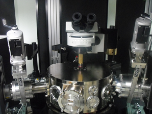
Figure 3: The 3TB4000 in position for on-line FIB nanofabrication and SEM imaging. (left) Location of AFM with respect to the SEM and FIB columns in the specimen chamber. (right) AFM probe tip imaged with the SEM. Image width = 210 µm.
Results
Improved Field of View
One interminable problem with SPM technology is the limited field of view. Thus, an immediate improvement in this limitation of SPM technology is seen in Figure 4 where one is able to zoom into a specific ZnO nanowire from a field of 600 µm to 40 µm. This has recently allowed the measurement of the optical attenuation coefficient of a particular ZnO nanowire using the near-field optical capability of this hybrid technology [9].

Figure 4: Zooming into a nanowire from a field of view of 600 µm to 40 µm.
Imaging an FIB Milled Trench
Figure 5a shows an AFM image profiling a 25-µm-deep trench with the large Z range of the system, both in terms of the scanner and the long exposed tip. The example in the figure is a trench milled in silicon with FIB. In this measurement, the FIB beam was used to mill this feature, and it was followed immediately by AFM imaging without having to remove the specimen from the FIB chamber and search for the feature of interest with the AFM. Furthermore, the true depth of the trench was measured by the AFM in a cross-sectional profile (Figure 5b), while a 3D reconstruction revealed the geometry of the sidewall (Figure 5c). Sidewall imaging with long and exposed tips becomes feasible with the 3TB4000 (see Figure 5c). The red arrow in this image clearly shows a Pt decoration on this structure, and the white arrow shows an undercut. SEM is severely limited in such imaging tasks.

Figure 5: Exposed side walls in a deep trench FIB-milled in silicon. (a) AFM topographic image, (b) AFM Z-height profile, and (c) 3D reconstruction showing the geometry of the sidewall.
In-situ Milling Measurements
The ability of AFM to quickly and easily follow FIB milling with high Z resolutionprovides a straightforward and convenient method for checking FIB milling results. This capability is demonstrated in Figure 6 where several FIB-milled features in Si were monitored during the milling process. The grayscale SEM image in Figure 6a can easily locate these features and measure their widths but cannot provide direct information on their depths. The AFM delivers an equivalent top-view image (Figure 6b), a 3D reconstruction (Figure 6c), and a cross-sectional profile(Figure 6d) that together provide a true topographic map of specimen features. The depth profiles demonstrate the linearity of the etching process with time.

Figure 6: Features milled in a focused ion beam (FIB). (a) SEM image, (b) AFM image, image width = 10 µm, (c) 3D reconstruction showing the cross-section, (d) cross-sectional profile along green line in (b) demonstrating the linearity of the etching process with time.
In-situ AFM Tip Condition Measurements
The benefits of AFM also can be seen in Figure 7 where the SEM image shows a fused silica AFM probe in contact with a surface under a controlled force. Figure 7a shows that the AFM probe is in contact with the surface, depressed, and even deformed by this interaction. In Figure 7b, the probe has been removed from the surface, and so it has relaxed and recovered its original shape without seriously affecting or compromising the tip shape. The SEM can be used to assess AFM tip condition at any point of the experiment, as shown in Figure 7c. An evaluation can be made concerning whether the tip has worn or been contaminated to the extent that it needs to be replaced. This adds validity to AFM measurements since there are often questions regarding the integrity of the AFM probe tip after any interaction with the surface. Furthermore, the lateral resolution in AFM is the convolution of the probe tip geometry with the sample geometry; this can now be directly assessed on-line at high resolution.

Figure 7: Monitoring the AFM tip with the SEM. (left) An AFM tip in contact with a surface, (right) assessment of tip condition with the SEM. If the tip has been contaminated during the imaging process, the FIB can be used to remove the contamination,and both the FIB and the on-line SEM can be employed to see the results of the cleaning. Figure 8 shows such a cleaning through imaging in top down images before and after cleaning (8a and 8b) and side view images before and after cleaning (8c and 8d).

Figure 8: Cleaning a contaminated probe. Top-down image (a) before and (b) after cleanin (image width = 43 µm). Side view images (c) before and (d) after cleaning (image width = 59 µm).
Material Property Measurements
In addition to important imaging tasks, the AFM is capable of measuring various properties of materials. One of these features, which is especially relevant in SEM and FIB, is the measurement of the elasticity within hybrid structures. An example of this measurement is shown in Figure 9 where the SEM was used to guide the AFM probe (Figure 9a). The AFM measures a lower elasticity in soft copper metal, which differentiates it from the surrounding stiffer silicon oxide in Figure 9b. The softer copper and the harder silica also have the effect of a trampoline on the probe; the probe experiences larger amplitudes on the harder surface. The line profile of the amplitude in Figure 9c was taken from the green cross-sectional profile in Figure 9b. The tuning fork in normal force mode hasamplitude as a measured parameter that is independent of the feedback. With such probes one can effectively monitor mechanical damping on-line without the need for digitization or further analysis of the intermittent contact mode amplitudes where the probe is contacting the surface at some defined frequency.

Figure 9: Imaging the elasticity of copper on silicon. (a) SEM used to locate measurement point, (b) AFM image distinguishes soft Cu (red) from stiff silica.
Monitoring Nanofabrication Processes
The FIB is increasingly used for nanofabrication with the requirement foraccurate Z control. The ability of an on-line AFM is useful in defining the effectiveness of such fabrication processes.
The Nanonics 3TB4000 incorporates innovations in the design and technology of atomic force microscopy enabling its integration with SEM and FIB technologies into a single powerful capability. Innovations in scanner design, probe manufacturing, and feedback loop have enabled this useful integration, resulting in a tool more powerful than its individual components. Several examples are shown where the SEM, FIB, and AFM are used together to provide complimentary information about the material. This will likely lead to the next generation of 3D functional analysis of devices, highlighting the disruptive nature of this technological synergism.
Videos
Watch SEM Movie of AFM Probe Scanning a Grating
Watch SEM Movie of AFM Probe Approaching a Surface
Professor Nancy Haegel: "Integrating Near-Field and Electron Optics: Dual Vision for the Nanoworld"