
SECM
SECM is a tool which is used to measure processes mainly in the vicinity of a surface. This technique can be used for fuel cells research, surface reactivity of solid state materials, the elucidation of enzymatic activities and other biophysical investigations. These all call for the probe to be in the near vicinity of the analyzed surface and to be able to control its spatial orientation.
The AFM-SECM combination enables one to track the topography in real-time at a fixed working distance while electrochemical signals related to surface activity are collected at the probe. The ability to add on spectrochemical analysis enhances this technique and can set new horizons to electrochemical investigations. Monitoring the Raman signal at real time gives the ability to understand the dynamics of the chemical reactions occurring at a sub-micron resolution in the vicinity of the SECM probe.
Nanonics systems provide unique liquid-based capabilities in scanning electrochemical microscopy (SECM) that now for the first time can be combined with other SPM methods such as AFM-Raman for chemical imaging together with the topographic and electrochemical current imaging. The Nanonics SECM capability incorporates Nanonics innovations in probe design, tip-sample feedback, and liquid cell design to enable new and revolutionary capabilities for the most advanced experiments.

Probes
Nanonics manufactures custom SECM probes with a continuous nanowire of platinum embedded in glass. A side view is seen below on the left left while a top view is seen below on the right clearly showing the platinum wire and glass. In the top-view, the white spot in the middle is the wire; the black ring around it is the glass.
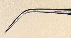
Side View of Probe

Top View of Probe
These custom probes provide simultaneous normal force sensing with full SECM functionality. Tip-sample feedback is maintained with the classic optical-based deflection method where a laser is reflected off the back end of this cantilever and directed towards a detector. Feedback can be maintained either via cantilever deflection or oscillation amplitude to keep the force, and hence tip-sample interaction, constant.
Liquid Cell / Environmental Chamber
Environmental Chamber
Nanonics provides a custom-designed liquid cell and environmental chamber to use in such measurements.
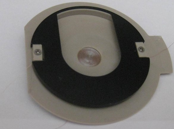
Liquid Cell Exposed
Sample is placed in ring in the middle. Changeable wire electrodes are on the sides.

Liquid Cell - Partially Covered
SECM Cell that is partially covered to minimize evaporation.
Liquid Cell - Bottom
Contains back contact for applying voltage to the sample.

Liquid Cell Design
The electrochemical cell is specially designed to protect from spillage.

Raman Integration
Nanonics systems feature full integration capabilities for real-time SECM measurements with AFM force feedback and simultaneous Raman measurements. The Raman setup through the laser, spectrometer, and CCD camera are placed above the probe with the optically friendly scanner and probe. Fluid measurements are observed using the critically important water immersion objective.
Nanonics MV2000 SECM-Raman Integration
Especially effective with water immersion objectives from above on opaque materials. (Pictured here with Renishaw InVia)

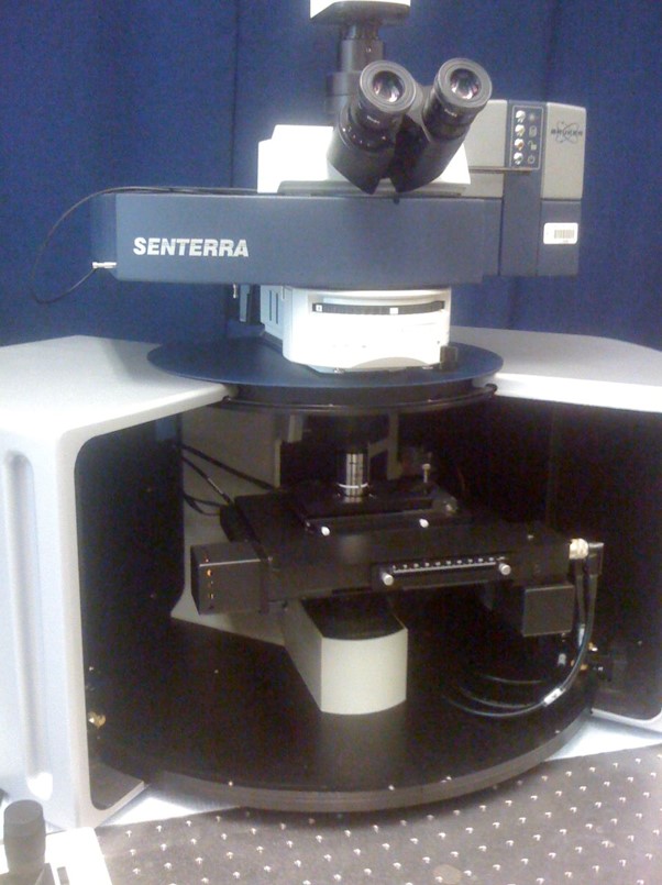
Nanonics MV2000 SECM-Raman Integration
(Pictured here with Bruker Senterra)
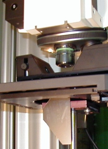
Nanonics MV4000 SECM-Raman Integration
Featuring multi-probe capabilities and unique Tuning Fork technology.
Nanonics MV15000 SECM-Raman Integration
Entry level with optical upgrade capability.

Applications
Simultaneous SECM current and Raman imaging of Copper during real-time etching
A silicon wafer with a thin layer of copper was used as the substrate for this electrochemical etching experiment. The SPM probe etched a small, ~4um hole within the copper layer, exposing the silicon substrate. Images of the substrate before (left) and after (right) the etching can be seen below with the etched point showing up as a dark spot in the right image.

The etching was monitored in real time with in situ Raman scattering where the Raman signature of silicon at 523 cm-1 was used to track the appearance of the silicon and thus progress of the etching process. A sample spectrum revealing the Si peak in the Raman spectrum is shown here:

Simultaneously, the current was monitored revealing a time delay between when the current was measured and when the exposed silicon was picked up the Raman spectra. This time delay was found to be dependent on the probe-substrate vertical distance.
3D collage of the simultaneously obtained AFM and SECM Images - Ferrocyanid

Colors correspond to the SEC signal; background corresponds to the topography
SECM probe in presence of 10mM ferrocyanide and 0.1M Na2SO4