Nanolithography
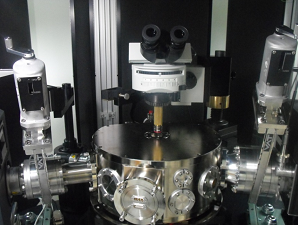
The field of ambient chemical nanolithography technologies was born in 1999 with two papers. One paper was based on the dip pen concept where to achieve the smallest writing dimensions a dry molecular ink was coated on an atomic force microscopy like probe [1]. This method was called dip pen nanolithography (DPN). A second paper was based on the concept of a fountain pen [2] and fully employed atomic force microscopy (AFM) and its feedback mechanisms but the writing element used was a nanopipette. This paper focuses on fountain pen nanolithography (FPN) and its evolution into a powerful generally applicable chemical writing method on many length scales with many surfaces and utilizing a wide variety of inks including gases. The technique in general uses a quartz cantilevered nanopipette with a tip highly exposed to the optical axis as seen in the figure to the right.

Figure 1: Diagrammatic representation of the Multiprobe Fountain Pen Nanolithography system
Quick Links
Introduction
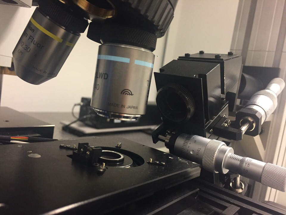
In the figure above and to the right: (a) Cantilevered glass probes with AFM sensitivity allow for a complete view of the probe tip which permits a direct view of the writing with a standard upright optical microscope and transparent integration with spectroscopic methodologies such as Raman for chemical characterization of the written structures. All cantilevered glass probes have exposed probe tips including those that can be applied for AFM, near-field optical, thermal, electrical and electrochemical nanocharacterization and so a wide spectrum of simultaneous multiprobe characterizaitino of the FPN process can be performed each with simultaneous independent AFM control of several tips. (b) Deposition can occur with a variety of inks and surfaces and can be controlled with voltage or pressure with other standard AFM parameters also adding additional control. The wetting interactions between the nanopipette, the ink and the surface are critical in the generality of the FPN process. Such an exposed tip has great advantages over other probe technologies where the tip is generally obscured from above by the cantilever
Figure shown to the right: A Generality of Results with FPN. (a,b,c) Deposition of CNTs in aqueous solution with surfactants. (a) CCD image of deposition on an n-type silicon substrate. (b) CCD image of deposition on SiO2 substrate demonstrating the capability of writing on previously deposited lines by FPN. (c) SEM image of deposition of carbon nanotubes on an organic PMMA layer covering an SiO2 substrate. . The line widths are 170-250 nm and cannot be seen by a regular optical microscope. (d) SEM image of depostion of 20% wt. of silver nitride in aqueous solution on 200 nm width gold structures lithographically imprinted on an SiO2 subtrate. (e,f) Writing lines of 40% wt. 50nm silver particles in Donol DB suspension. (e) CCD image of writing lines on 1.5 micron width of gold structure lithographically deposited on an SiO2 substrate. (f) CCD image of lines that were written from a gold surface to an SiO2 substrate. The conductivity of the lines in this latter deposition were investigated and were of high conductivity.

Figure 2: A generality of results with FPN.
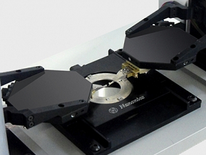
Another aspect of this attribute is that it allows for multiple independently controlled probes to be brought within touching distance of the multiple tips (see Figure 1a) [4]. As a result, one can have in one or multiple probes writing nanopipettes, while an alternate probe can be used for on-line high resolution imaging and writing characterization. Furthermore, other functional probes such as electrical, thermal, electrochemical and Kelvin probes can also be on-line to investigate the writing process at different time points. A movie of FPN with multiprobe AFM characterization can be seen on the web In FPN it is becoming increasingly evident that its generality arises from critical wetting interactions between the ink and surface that is chosen (Figure 1b). For comparison, in DPN the molecules are delivered to the surface through a water meniscus and the deposition rate is dependent on the diffusion rate of each molecule. This process has drawbacks since each molecular ink is limited only to its corresponding substrate, the diffusion process is relative slow and the method only works in contact with the surface. In FPN there are several important parameters that readily allow for control of the ink deposition. One such parameter is the induction of pressure by either imposed voltages over the column of liquid [6], or the imposition of a defined pressure from the back of a liquid column. In the case of gases this pressure can be differential between the inside of the pipette and the surrounding environment (see Figure 5). In addition to such control, several AFM parameters also have an influence on the writing, namely the nanopipette aperture, the speed (see Figure 5), the imposed force of the tip to the surface (set-point) (see Figure 6), the mode of AFM operation (contact or non-contact) etc. Generally the humidity effects are not as critical as in DPN which depends on an aqueous bridge that arises from the surface wetting. Presently, knowledge is rapidly accumulating in the FPN field that allows for the effective use of the generality of the method in numerous areas of fundamental and applied science. This article is aimed at leading the reader to an understanding of these advances.
Materials & Methods
Probes and Feedback
The probes used were glass cantilevered nanopipette capillaries with diameters that varied from 35 nm to 10 microns. These probes were used either with beam bounce amplitude feedback or complexed to tuning forks for implementing tapping mode normal force tuning fork operation. Tip approach, feedback and scanning are under atomic force microscope control. As noted above both contact and non-contact AFM can be used with FPN. The advantage of non-contact is that one can consider writing on very soft surfaces which would be difficult to access with contact mode operation. In addition, tuning forks allow for true non-contact operation. This is difficult to achieve with beam bounce silicon cantilever methodologies due to jump to contact instabilities in AFM silicon probes when they approach less than ~10 nm above the surface. In tuning forks, this unique behavior of no jump to contact and no adhesion ringing is achieved due to the much stiffer (>3 orders of magnitude) force constants of 2,600 N/m relative to silicon AFM cantilevers. This stiffness gives tuning forks the attribute of ultra sharp frequency spectra with high Q factors and associated force sensitivity that permit feedback based on frequency modulation. In addition, such high Q factors, when complexed to glass probes that by themselves are relatively stiff with a few N/m force constants, allow for the ultimate in force sensitivity for glass based probe technology. This is achieved by the sharp frequency spectrum that permits frequency and not amplitude as a monitor of the force. In fact, it has been demonstrated, that with such a combination of tuning forks and glass probes, a force sensitivity of 1.6 pN can be reached, which is much higher than what can be achieved by the best beam bounce technologies available today[7]. Therefore, the ultimate in force microscopy can be readily integrated with the chemical writing process and this is presently in its infancy in FPN. Both this aspect of sensitive force detection with no jump to contact and adhesion ringing allow for relatively difficult tasks such as writing on, for example, thin carbon membranes that are found in certain transmission electron microscopy grids.
Results
The results shown in the figures demonstrate the generality of inks and surfaces in the FPN writing process as indicated above. In Figure 2 different surfaces, different inks and different dimensions are all shown. Even the ability to write with liquid inks on structures previously written by other lithographic processes is demonstrated and the ability to over-write structures previously written by FPN is shown for the case of the Star of David in Figure 2b. A movie of this latter writing process can be viewed on the web [8]. Inks>: Carbon Nanotubes, Salt Solutions & Nanoparticle Suspensions Surfaces: n Type Silicon, Si02, Organic Photoresist & Gold InFigures 2a-c, the ink was a suspension of carbon nanotubes (CNTs) in an aqueous suspension with 1% wt. of sodium cholate. In Figures 2a and b the writing could be accomplished on n type silicon and silicon oxide surfaces. In Figure 2c, the CNTs are written on an organic electron beam photoresist layer. In Figure 2d an aqueous salt solution with 20% wt. silver nitrate is the ink while in Figure 2e and f a silver nanoparticle (50 nm dimension) in Downol DB suspension (Gift from Xjet Solar Ltd, Israel) is written. In Figure 2d and 2e, the solution and the suspension respectively were written on gold lines. In 2d the previously written lithographic structures had dimensions and separations that were too small to see in the optical microscope as resolved features but were clearly visible in the scanning electron microscopy image shown.In Figure 2e even previously written structures by other lithographic processes on the 1.5 micron level could be targeted and written on, due to the completely free axis from above as a result of the probe and SPM system geometry.. In Figure 2f, the writing across an interface between the gold and the SiO2 allowed for an AFM electrical probe to be placed on the SiO2 end of the written structures for the measurement of conductivity of the line with a counter electrode on the gold pad.
Control of the Writing Process : Voltage
The control of the writing process with FPN by imposed force of voltage or pressure is seen next in Figures 3-5. For the voltage control the nanopipette with its insulating glass walls allows for a variety of voltage options to be provided as indicated in Figure 3a.
figure 3: High resolution voltage controlled nanoprinting of 1.4 nm gold nano particles on n type silicon. (a) Variety of voltage controlled nanoprinting options. (b) 2D AFM image of an array of nanoparitcles written with a 50nm pipette. (c) 3D AFM image of the written array with a 35nm pipette. (d) line scan of the image in c showing feature sizes of ~ 40 nm due to a convolution of the 20 nm AFM tip used. An average height of single nano-particles of 1.4 nm seems to indicate that individual gold nanoparticles were deposited as per the dimension reported by the supplier of these particles. Figures 3b-d, 4d-g show deposition of 1.4 nm gold nano particles (Nanogold®, Nanoprobes, Yaphank, NY, USA suspension in an organic solvent which in this case was methanol (1 mg/ml). Voltage was shown to work even with such an organic solvent. The voltage control allows for the use of pipettes with dimensions as small as 35 nm that are difficult to use with regular FPN. The best resolution can be seen on Figure 3c and d when a 35nm nanopippete wrote dots with diameter of 40nm and average height of 1.4nm which is the height of the single particle that was used.

Figure 3: High resolution voltage controlled nanoprinting of 1.4 nm gold nano particles on n type silicon
Controlled Writing On Rough Real Substrates
The above writing was affected on generally flat surfaces. In Figure 4 the ability to accomplish complex tasks on rough surfaces with pressure control are shown. An example is the filling of a photonic band gap crystal with the fluorescent labelled protein BSA (Figure 4a).The subsequent near-field optical fluorescent image is shown in Figure 4b. Photonic band gap crystals guide light and are very sensitive to perturbations in their structure. The ability to affect such perturbations selectively using FPN is an important attribute that has many potential applications in photonics.An additional example also shown in Figure 4 is the demonstration of filling a deep trench with a suspension of 1.4 nm gold particles. The task accomplished in this case was the filling of a via with pure gold so that an effective contact could be made with the copper contact shown at the base (Figure 4c). The high aspect ratio of the nanopipette probes are very effective in this task and the results of the filling operation are shown in Figure 4 f and g.
Figure 4: Controlled nanoinjection in holes. (a) SEM image of florescent protein deposition in a single hole of a 1.5 micron photonic band gap with pressure control. (b) On-line near-field optical characterization of the fluorescent bovine serum albumin (BSA) that filled the holes of this silicon photonic band gap material. (c) Illustration of the injection to a 0.5 X 0.5 µ2 hole. The challenge was to fill this via with pure metallic nano particles. (d) 3-D AFM image of the hole before the injection. (e) Height profile along the blue line indicated in panel d shows that the depth of the hole to be 2.3µm. (f) 3-D AFM image of the hole after the voltage injection of 1.4 gold nanoparticles in methanol solution. (g) Height profile along the 1.4 µm green line indicated in panel f shows the depth of the hole to be 1.4 µm after injection.

Figure 4: Controlled nanoinjection in holes
Control of the Writing Process
The use of differential pressure in the controlled evolution of an ink is clearly shown in Figure 5. In Figure 5a the use of pressure to evolve gas in an aqueous medium is clearly evident while in Figure 5b and c, slits in a polymethylmethacrylate (PMMA) layer were accomplished with a nanopipette through which acetone vapor was effectively effused. The depth of the etching of the PMMA is clearly dependent on the speed of the relative motion of the nanopipette over the surface. These are the first examples of AFM controlled gas chemistry on a surface [9]. In addition, such pressure effects are of crucial importance in the AFM controlled deposition of macroscopic objects such as single cells and shown in [10].
Figure 5: Nanowriting with gases. (a) Using pressure to evolve air in an aqueous medium. (b) AFM image of slits in a PMMA layer etched using acetone vapor delivery through an 800nm pipette. The velocity of the tip scanning was changed as indicated above each line. (b) Cross section through the lines in panel b.

Figure 5: Nanowriting with gases
Set-Point:
In Figure 6 another AFM parameter is altered and its effect on the line widths of different materials on different surfaces are compared. In Figure 6a, 50nm silver particles were written with the same pipette and conditions except that the set-point of the nanopipette was altered. It can clearly be seen that the larger force between the nanopipette and the surface led to higher particle concentration on both the Au and SiO2 surfaces across which the writing took place. An electrical AFM probe was placed on these lines with a second contact on the Au surface and the conductivity was measured. The written line at the extreme left of this image visibly had the largest concentration of particles and showed the highest conductivity. In Figure 6 b and c the ultimate resolution of writing BSA in aqueous media, using non-contact mode on a glass surface with low set point is shown and the line widths are between 50-100 nm. Note that such FPN protein writing [11] can be accomplished without protein modification which is difficult to accomplish with DPN.
Figure 6: Controlling The Line Dimensions With Different Set-points. (a) AFM image of lines written with different set-points with an ink of 50nm silver particles between the interface of a gold and SiO2 substrate. The highest conductivity was measured on the line with the largest concentration of nanoparticles as seen in the AFM image. (b) deposition of unmodified BSA protein on glass in non-contact mode with low set-point. (c) Line scan of the lines in panel b. showing a width: 50-100nm.

Figure 6: Controlling the line dimensions with different set-points
Conclusion
The generality of the writing process with FPN as has been noted, is based on the manipulation of the wetting process on a nanometric scale. This is a multifaceted problem both from the practical aspects of the FPN and from the fundamental aspects of such processes on a nanoscale. An excellent review has recently appeared [12]. From the point of view of the practical aspects of FPN, there are the issues of how a liquid column emanating from the tip of a pipette wets the surface that is to be written on. However, there is also the question of the wetting behavior of the nanopipette itself. For example, how does the surface on the inside walls of the nanopipette behave vis a vis the solvent that will be used for the writing? Or, what is the nature of the outer walls of the pipette? >In addition, from the perspective of the surface there is certainly the issue of whether the surface is hydrophobic or hydrophyllic or represents some intermediate state. But even these basic questions have to be complexed on the nanoscale with the roughness of the surface. Basically, roughness amplifies wetting behavior and such wetting behavior is best described by the contact angle. The contact angle is defined conventionally as the angle at the point where a liquid/vapor interface meets a solid surface (see Figure 7a). It quantifies the wettability of the solid surface. Thus, the issues of FPN nanowriting are at the forefront of nanotechnology both from an experimental and computational perspective. Thus, there is enormous fundamental work that can be accomplished in this area using the FPN technologies described in this paper..
Figure 7b and 7c show the effect of such wetting using an aqueous solution of 20% silver nitrate deposited on gold with 200 nm nanopipettes. A wetting agent BYK348 was added to the solution. When the concentration of the wetting agent was 0.003% wt. a contact angle of 65 with the gold substrate was measured and for such a contact angle lines of 80-110nm width were obtained as shown in Figure 7b. This was less than the orifice of the pipette used. On the other hand, the same pipette with the same solution but with 0.005% wt. of BYK348 gave a contact angle of 50+80 with the gold substrate and the lines were 600-700nm in width (see Figure 7c), more than the nanopippete aperture. Finally, when the concentration of the wetting agent was 0.001% wt, the contact angle was 78and no writing took place. Finally, we should note that chemical characterization of the process of FPN is of great importance as we move forward. Thus, nanopipettes and all glass based probes, that have the attribute of exposed probe tips, allow with the SPM platforms we have employed a completely clear optical axis from above and below for full integration with techniques such as Raman spectroscopy. Using on-line Raman one can understand the chemical changes occurring during the writing but one can also understand both the chemical structure of the written pattern. A most appropriate example is a recent initial study that has shown that carbon nanotubes written by FPN on silicon oxide sitting on a bulk silicon substrate are highly oriented [13]. Further work on fully quantifying this effect is underway in our laboratories which has import both in the deposition of other forms of nanorods and in controlled polymer deposition that has been used to create polymer lenses for nanobiochip applications [14].
Figure 7: Controlling The Width of FPN Written Lines With Different Contact Angle. (a) illustration of the contact angle between a surface and a liquid droplet. (b,c) AFM images of the deposition of 20% wt. silver nitride in aqueous solution on a gold substrate with a 200 nm orifice nanopipette (b) 0.003% wt. of the wetting agent BYK-348 was added. This solution gave a contact angle of 65+50 with the gold substrate. The resulting lines had a width of 80-110 nm, less than the nanopippete orifice. (c) 0.005% wt. of BYK-348 wetting agent was added. The solution gave a contact angle of 50+80 with the gold substrate. The lines were 600-700nm width, more than the nanopippete aperture.

Figure 7: Controlling the width of FPN written lines with different contact angle
Summary
As can be seen, the application of FPN is diverse and has already matured in many important directions. However, the future is also very bright and some of the seeds of that future are already either in the germination form or are actively prevalent in the writings of those who have actively considered the technique. An example of the former is the controlled deposition of catalytic particles [15]. An example of the latter is the important chromatography that was already noted earlier in the literature [16]. This could combine nanodeposition with chemical separation. Finally, the AFM systems and probes used in the work reported in this article are also able to be inserted into scanning electron microscopes and SEM/FIB systems [17]. Thus, the ability to, with AFM control, deposit gases or multiple gases with a high degree of local control could materially affect the quality of electron beam based lithographic methodology which presently has to fill the vacuum chamber of the SEM/FIB with specific gases for writing with electron and ion beams.
Videos
Drawing Single Walled Carbon Nanotubes on Si02
Drawing Single Walled CNT Electrode Interconnections
Nanolithography with Online AFM Imaging
Deposition of Protein Nanoarray
Writing of a Protein
Deposition of Ultra-thin BSA Protein Lines on Si Surface
Filling & Preparing the NanoPipette Probe