AFM SEM/FIB
Integrated Nanoscale Characterization

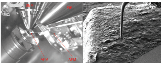
The AFM SEM/FIB is an award-winning SPM/NSOM system seamlessly integrated with SEM/FIB. This instrument is based on a revolutionary design that provides open access to the SEM/FIB beams for complete integration of SPM, SEM and FIB. The SPM probe does not obscure the electronic or ion beam axis and also sits at the eucentric point, enabling the SPM to rotate into position while either the electron or ion beam is in operation.

Key Features
- Simultaneous imaging of surfaces with SEM/SPM
- True 3-D functional imaging by taking advantage of ion beam milling
- Excellent X,Y resolution of SEM coupled with ultimate Z resolution in SPM
- NSOM imaging within an SEM
- Large field of view screening with SEM, followed by high resolution SPM imaging
- Functional nanoscale imaging taking advantage of SPM/NSOM imaging (e.g. cathodoluminescence, electrical, force)
- Innovative probe design that does not interfere with electron axis
- Multiprobe SPM Imaging and manipulation
- Unique AFM capabilities of Deep Trench Profiling and Side Wall Imaging
- Super-resolution optical imaging inside SEM/FIB such as cathodoluminescence
Product Design
On-line Scanned Probe Microscopy Transparently Integrated with Twin SEM/FIB Systems
There are several technology challenges to overcome to obtain a transparent SPM integration within the limited space of a combined electron/ion beam system without perturbing any detectors or nanomanipulators that can be incorporated into such systems.
A series of Nanonics innovations available with the MultiView SPM series allow for electron & ion optical friendly SPM integrations and with the probe tip at the eucentric point and rotatable for on-line FIB or SEM imaging, as shown on the right image. The open access above the AFM probe enables both the FIB and SEM beams to be positioned on top or on the side in a geometry that accomodates all three beams.
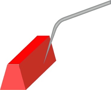
A different view of the geometry around the tuning fork is shown below, clearly showing the open access to the tuning fork based probe. Because there is no optical lever detection system for monitoring tip-sample feedback, which is instead done through tuning fork actuation, the AFM cantilever has an open geometry around it for the SEM and FIB beams. An SEM view of the AFM probe is also shown below.

AFM/SEM/FIB Configurations
Nanonics MultiProbe SPM systems are available now inside SEM/FIB chambers. Up to four SPM probes, all in active AFM feedback can be brought into close proximity with free electron and ion optical axes. The integration into SEM/FIB has different configurations:
 |
 |
|
MultiView 4000/SEM/FIB Single probe door mounted |
MultiView 4000/SEM/FIB Single probe door mounted scheme |
 |
 |
|
MultiView 4000/SEM/FIB Two probes stage mounted |
MultiView 4000/SEM/FIB two probes stage mounted (close up). |
AFM/SEM/FIB Specifications
- Probe & Stage Scanning (Door mounted only probe scanning)
- X & Y range 70 um (Door mounted)
- X & Y range 150 m (Stage mounted)
- Z range 35 um (Door mounted)
- Z range 115 um (Stage mounted)
- Sample Z autofocus to keep tip & sample in E beam focus (N/A door mounted)
- Standard silicon cantilevers
- Unique glass cantilevers & NanoToolKitTM of SEM/FIB friendly probes with a variety of functionalities from electrical to thermal to near-field optica
Applications
AFM SEM FIB Applications
Resolving SPM Problems
Online AFM/SEM/FIB integration solves problems of scanning speed of SPM. SPM scans at a snail's speed compared to an FIB or SEM. Taking advantage of this fast speed, SEM allows for rapid SPM probe placement in a large field of view provided by the SEM and available with the exposed probes.
|
|
Exposed AFM probe shown within the SEM field of view |
AFM 3D Functional Monitoring of FIB etching
On the other hand, AFM/SEM/FIB integration overcomes SEM/FIB problems of monitoring depth or Z topographies of an etched area performed by the FIB. The ultra-sensitivity of the AFM allows for precise monitoring down to sub-nanometers 3D functional imaging of etching affected by the FIB.
 |
FIB etching indicated by red arrow |
 |
 |
|
3D AFM image of the etched area above |
Height profile of the etched area (green line on left image) |
Material Contrast in a SEM/FIB
Tuning fork AFM allows for new directions in material contrast with FIB etching. Amplitude signal of the tuning fork, in phase feedback mode, provides elasticity monitoring of the imaged features.
 |
|
|
(Left): A snap shot of AFM imaging of Copper feature on Oxide surface presented through an SEM image. Transparent optical axis of glass probes allows free electron axis for viewing and accurate positioning of the AFM tip. (Right): Elasticity image performed trough Amplitude signals which show different level of signals on different materials. The softer (Copper) provides lower amplitude. |
|
Probe Integrity - Processing & Repair
SEM allows for online monitoring of AFM probe/tip characteristics. The following SEM images show the probe behavior and the tip characteristics under high pressing on the sample with large setpoint.
 |
 |
 |
|
SEM image shows a high pressing of an AFM probe (mounted on tuning fork with normal force sensing) with large sepoint. |
SEM image of the probe after retraction |
High resolution SEM image shows the tip end after the retraction. (bar is 50nm) |
Furthermore, FIB adds unique functionalities if tip probe integrity such as modifying the AFM tip as shown in the following pictures.
 |
 |
|
Silver paint attached to the end of the tip |
Cleaning the silver paint at the end of the tip by FIB |
Deep Trench Profiling
Trench profiling is a must for FIB etching for monitoring quality of the etching. Standard AFM systems fail in profiling deep trenches due to limitations of Z range and tip's aspect ratio. Nanonics SPM systems provide large Z range of up to 170 microns and cantilevered glass probes with high aspect ratio.
 |
 |
|
Nanonics probes with high aspect ratio and large Z range are ideal for deep trench profiling. |
3D AFM image shows deep trench's topography. |
Side Wall Imaging
In addition to deep trench profiling, Nanonics SPM systems integrated inside SEM/FIB allows other unique capabilities such as side wall imaging. Side wall imaging enhances SEM/FIB with additional imaging perspectives.
 |
 |
|
Nanonics probes with high aspect ratio and large Z range are ideal for side wall imaging. |
Side wall AFM imaging |
Cathodoluminescence
Nanonics SPM systems provide unique solutions for near-field imaging with cantilevered fiber probes. Super-resolution near-field optical imaging in a SEM with topographically correlated cathodoluminescence is available now in AFM/SRM/FIB integrations.
 |
 |
 |
|
Near-field Cathodoluminescence from a GaN nanowire under ion beam excitation inside an SEM chamber. On-line AFM (left) and NSOM (middle) images obtained in collection mode. The NSOM image shows an evanescent light decay along the nanowire and light distribution at the nanowire output. Collage AFM/NSOM is shows on right image. |
||
NanoToolKitTM Probes
A variety of Nanonics cantilevered probes with exposed ion/electron axes are suitable for SPM/SEM/FIB integrations. Among these are electrical/thermal/NSOM/nano-heaters and other functional probes. Furthermore, these probes are suitable for multiprobe SPM imaging and nanomanipulations
AFM-SEM Comparison
AFM-SEM Comparison Chart
| Characteristics | AFM | SEM |
| Field of View | Small ~0.1mm | Large ~mm |
| Speed | Slow | Fast |
| Surface structure sensitivity | Similar to SEM | Similar to AFM |
|
Surface rougness |
Better in AFM to 0.1nm | Worse in SEM |
| Vertical resolution | Better in AFM to 0.1nm | Worse in SEM |
| Lateral resolution | Similar to SEM | Similar to AFM |
| Optical measurements | Near-field and Far-field available | Only far-field available |
| Electrical measurements | Available | Not available |
| Magnetic measurements | Available | Not available |
| Thermal measurements | Available | Not available |
| Subsurface imaging | Available with thermal conductivity and near-field | Not available |
| Deep trenches with high aspect ratio structures | Possible with Nanonics specialized probes | Not available |
| Sidewall imaging | Possible with all Nanonics probes | Not readily available |
| Undercuts | Possible with Nanonics specialized probes | Difficult to not available |
| Elemental analysis | Not available | Available |


