
Seamless Integration of AFM and Confocal Raman With Proven, Award-Winning Tip enhanced Raman spectroscopy (TERS)
From The Pioneers: Nanonics Imaging's pioneering efforts in the integration of AFM and Raman began over a decade ago in 1999 with the first installation of such a system with a commercial Raman spectrometer in Chalmers University of Technology in Sweden. From this beginning, a Nanonics system was used in 2001 for the first Tip Enhanced Raman Spectroscopy (TERS) publication with a commercial system. This publication used a unique probe developed by Nanonics that provided high dielectric contrast gold nanoparticle glass probes with no Raman background. Since then, installations of Nanonics' singular offerings of this combination of imaging modalities have occurred throughout the world. Nanonics systems are viewed as the most synergistic combination of AFM with optics with its integration of all forms of AFM with Raman being a "jewel in its crown". Leadership in innovation was and is needed for the continual evolution of this technique and Nanonics through its focus on innovation and excellence has evolved a MultiViewTM scanning probe microscopy product line with singular capabilities hallmarked by non-interfering seamless integration, proven TERS, a NanoToolKitTM of Raman friendly and Multiprobe friendly Full ViewTM functional OptoProbesTM which make Nanonics the leading supplier of AFM Raman/TERS in the world. The list below is a summary of these unique features of Nanonics AFM Raman/TERS systems designed from the bottom up from unique technology in the microscope to singular technology in the probes.
A video of how TERS operates on Nanonics systems can be found here on our YouTube Channel.
For additional info, please contact us at info@nanonics.co.il or visit our contact us page.
Key Features
Seamless Integration of AFM and Raman With Proven Tip Enhanced Raman Spectroscopy (TERS)
One head fits all
- AFM Systems that can be placed on any Standard Unmodified Upright, Inverted & Even Simultaneous Upright/Inverted Dual Optical Microscopes
- Place directly on any microRaman stage with complete isolation from Raman noise sources
- No need for multiple or different heads for different microscopes
- Completely free optical axis from above and below
- Or place on a separate integration package for the ability to perform measurements on two separate samples at the same time
- Integration packages allow for on-line upright and inverted dual microscopes with Raman AFM thus permitting reflection and transmission Raman in the same package
- Readily investigate opaque or transparent samples from above or below with the innovations resulting from ‘one head fits all'
Interference free AFM
- All probes with exposed probe tips & non-interfering cantilevers that are high (>60 m) and out of the optical focus of the tip
- Be they AFM or Even Functional Force Sensing Probes for Electrical, Thermal, Electrochemical, Optical, Ion Conductance or NanoChemical Deposition
- AFM feedback with no laser optical background interference
- Switch at will to any Raman excitation laser available
- No complications of laser feedback through Raman objective
- Allowing synergistic AFM & Raman with no cross interference
- Ultimate in On-line AFM Autofocus resulting from a non-interfering probe and a large Z range (upto 100 m) sample scanner feedback
- Rigidly maintains sample surface to lens distance for every pixel yielding artifact free Raman chemical mapping
- Autofocus with large Z range also permits for exceptional 3D AFM Raman mapping
Known advantages of normal force tuning force feedback fully implemented in air and liquid
- Stiff cantilevers with no jump to contact even at <1 nm permitting with the same probe AFM & tunneling gap mode investigations
- Ultrasensitivity with ultrahigh Q factors having ultra sharp resonances
- All the advantages of frequency modulation
Patented tuning forks fully immersed in liquid without the loss of high Q factor advantages of tuning forks
- Permitting ultra high numerical aperture water immersion objectives from above with AFM sensor in place
- Maximizing Raman signal while doing AFM even on opaque samples
- The smallest working distances from above ever achieved by an AFM system, 3.5 mm with highest numerical apertures in upto 100x objectives
A Decade of Proven TERS
- Patented exposed tip probes with unique gold nanoparticles in glass with high dielectric contrast & no Raman background
- All systems with probe scanning for optimal & rigid probe placement in Z polarization & excellent difference Raman for resolving near-field from far-field without sample movement. No need for any translational of any Raman excitation optical elements for optimal relative probe/beam placement.
- Sample scanning on-line AFM based autofocus reducing noise
- Ultimate TERS sensitivity and artifact removal
- No laser feedback TERS background
- Published work on the most complex systems such as proteins
Multiprobe AFM Raman
- Dual TERS exposed gold nanoparticle probes for gap modes without STM
- On-line electrical conductivity with Raman even on insulating substrates such as grapheme on silicon
- On line nanoheating and temperature measurements as a function of distance with Raman chemical mapping
- On-line dual oxidizing and reducing scanning electrochemical microscopy probes with Raman chemical mapping
Complex of chemical microscopies in the same AFM Raman head just change the probe
- Near-field scanning optical microscopy in reflection, transmission, collection mode and fluorescence with fluorescence spectroscopy.
- Confocal fluorescence spectral imaging
- Scanning electrochemical microscopy with on-line normal force AFM feedback
- Ion conductance imaging with on-line normal force AFM feedback
- Kelvin probe
- Thermal conductivity
- Nonchemical Fountain Pen nanolithography with closed loop scanning
- All of the above with a singular NanoToolKitTM of exposed probe tip/non-obscuring cantilever Full ViewTM Probes patented by Nanonics
Unique AFM features not found in standard AFM Raman systems
- Ultra large Z range upto170 m
- Deep trench high aspect ratio AFM imaging of semiconductor structures with Raman chemical mapping
- Side wall AFM imaging of semiconductor and other structures
- Millimeters of rough scanning without the need for additional rough stages
- On-line lensed fiber illumination at any angle for different protocols with on-line Raman AFM
- Independent placement of probe and Raman excitation point for flexibility of on-line perturbation
- Environmental chambers with glove box compatibility and free optical axis from above and below for seamless Raman AFM integration
- Vacuum and temperature controlled options
- The first temperature controlled AFM sample scanning liquid cell for biological applications
- Tight compact designs for very low drift even at variable temperatures
All of the above while still permitting if desired often repeated modes of AFM with their known difficulties
- Beam bounce with on-line tuning fork feedback
- Silicon cantilevers
- Off-axis Raman illumination due to the obscuring geometries resulting from beam bounce and silicon cantilevers
Design
Seamless Integration of AFM and Raman
Innovations over Standard AFM Technology for Transparent AFM Raman Integration:
Variety of SPM technology innovations of Non-Obscuring UltraFlat Scanners, exposed cantilevered probes and non-interfering tuning fork feedback allow for transparent integration of Nanonics SPM systems with all types of optical and Raman microscopes including Upright, Inverted and Dual Optical Microscope configurations.
The following list presents Nanonics SPM innovations for successful online AFM/Raman/TERS integrations.
| Standard AFMs |
Nanonics Innovative SPM Technology |
| Obscuring Piezo tube scanners | Non-Obscuring UltraFlat Scanners (Nanonics 3D FlatScanTM scanning stages) |
  |
|
| Obscuring Probes | Exposed Cantilevered Probes |
 |
 |
| Beam-Bounced Feedback technology | Non-Interfering Tuning Fork Feedback |
 |
 |
| -Imposes geometrical constraints -Imposes Optical background |
- Friendly geometry for optical integrations with short working distance from above |
Unique AFM/Raman/TERS Integration:
- Integration with all optical microscopes: Upright, Inverted and Dual microscopes
- A transparent probe with no Raman background
- Ultimate in feedback without any optical interference
- Specialized scanning modes optimized for Raman including Tip & Sample Scanning operation
- Ultralow working distance from above including, for the first time, the use of water
immersion objectives with same-side upright microscope AFM - Optimized TERS with single gold nanoparticle probes and tip-controlled difference Raman
- All modes of TERS/SPM/NSOM possible with one system
- Innovative Multiprobe Scanned Probe Microscopy systems
AFM Raman
Direct Correlation of Raman and SPM Imaging
By placing a Nanonics AFM NSOM microscope with its free optical axis, onto a standard Raman microscope, for the first time it is possible to integrate the separate worlds of Raman and AFM.
- Award-winning design
- Single SPM/Raman software package
- NSOM enhanced Raman techniques
- Large scan range 200um in the XY plane
A Breakthrough for Raman Spectroscopy
Although Raman scattering is currently undergoing a renaissance, it thus far has remained separate and removed from the proliferation of insights that Scanned Probe Microscopies (SPM) can give. In general, investigating a sample with scanned probe microscopies requires removing the sample from the micro-Raman spectrometer. This means that the exact region that was being interrogated by Raman cannot be found again for the chosen SPM imaging technique. Direct correlation of Raman scattering with an SPM technique has been a dream.
Transparent Correlation of Raman and SPM Imaging
|
The Nanonics MultiView 1000™ system can be directly integrated into the Renishaw RM Series Raman Microscope. These microscopes employ the upright microscope configuration, and the Nanonics MultiView 1000™ is readily placed on the sample stage of such a microscope (see picture). All other systems combining AFM and Raman perform seperately either an AFM scan or a Raman scan. No system other than the Nanonics-Renishaw combination provides simultaneous and on-line data from both modalities. This enormous advantage resolves critical problems in Raman such as intensity comparisons in Raman images and provides for new avenues of improved resolution as described below |
 |
AFM without Optical Obstruction

The Nanonics patented cantilevered optical fibers are held between the microscope lens and the sample without obstructing any aspect of the Far-field optics. The tip in these fibers is exposed and illuminated by the lens of the microscope, allowing the user to view the exact region where the SPM and Raman information is being collected.
Parallel Imaging
With the combined system, one can now record, in parallel with Raman, a wide variety of scanned probe imaging modalities. For example, while the Si Raman peak of a microcircuit is being monitored to detect stress in the silicon, the Raman spectroscopist can simultaneously measure the circuit's micro-topography with AFM, and its NSOM reflectivity or its electrical properties, such as the dopant concentration. In addition, Nanonics provides software that can display all these images at once for direct and simultaneous comparison and analysis.
 |
 |
|
Parallel imaging of a Silicon Semiconductor |
High Resolution Raman Mapping with Z-feedback Conventional Raman Mapping
|
There is a serious drawback to Raman Spectroscopy when studying non-smooth surfaces. As with all lens-based microscopy techniques, Raman suffers from the problem of out-of–focus light. When a sample is scanned conventionally under the illuminating beam of a Raman microscope, the uneven sample surface will scan in and out of the focal plane. As a result the resolution of the Raman mapping is limited by the large area of the unfocussed beam on the sample. In addition, the point spread function is significantly broader where there are contributions from the out-of-focus light. |
 |
As a result the Raman spectra of non-flat surfaces can be very misleading, and tend to misrepresent the true information that could be gained by using Raman.
Raman Mapping with Z-Control
| The problem of out-of focus light can be solved by using a Z-feedback mechanism. With this feedback in place the surface of the sample can be kept in the focal plane throughout the scan. All the Nanonics MultiView AFM platforms have completely free optical axis. This makes them the ideal add on to any Raman system to provide the Z-control necessary for true high resolution Raman mapping. |
 |
Examples of the Power of Integrated Raman/AFM
The difference between Raman mapping with and without Z-control can be seen clearly in the examples below. Here the vibrational mode of diamond is represented:
The Vibrational Mode of Diamond at 1334cm-1
|
|
|
 |
 Without Z control
The pair of images on the left shows the same area mapped with and without Z-control. The advantage of Z-control is made apparent by the differences between the two.
The image on the right is a collage of AFM topography and Raman intensity of the same sample at two different wavelengths. Note the differences in the intensity of the two images. For example the bright spots at the top of the image at 1334cm-1 which are absent from the image at 1525cm-1.
No other Raman system has sufficient control of Z position to pick out these differences.
Nanoindentation Correlated with Material Properties
To illustrate this combination of the worlds of AFM and Raman spectroscopy, actual data has been obtained on the Si stress problem mentioned above. A 14 x 14 micron AFM height image of a nanoindentation in Si is shown here (figure a) with a line scan (figure b) through a region of this AFM image.

The points on the AFM cross section are points at which Raman microscope spectra were collected. As a result of the nanoindentation, it can be seen that the silicon has been displaced. The question is whether or not these regions correspond to different phases of the silicon that can be correlated with the AFM measurements. Only Raman microprobe spectroscopy can give this information. The Raman spectra were obtained at the same time as the topography was being measured.
Local Stress of MEMs Devices
Raman spectroscopy is a most important technique for measuring silicon strain. On-line AFM can impose finely controlled and well defined strain on silicon with pressures exceeding megapascals since the area of a probe tip is nanometric NanoRaman technology is the ideal for super-resolution silicon stress measurements in floating structures such as combs and forks.
The on-line AFM allows for defined forces to be imposed on a MEMs cantilever while the on-line Raman measures the shift in the silicon vibrational frequency & silicon strain at the cross (see below). No other AFM is capable of such a combination.
|
|
|
|
|
|


Raman Shift as a Function of Local Stress Location |

Intermittent Contact Mode in Liquids
In addition, the joint Nanonics/Renishaw Raman and SPM system can operate in intermittent contact mode even in liquids. Thus, the whole world of NSOM/SPM imaging of biological materials in physiological media can now be directly correlated with Raman spectra.
Configurations
AFM Raman TERS Configurations
Nanonics MultiView SPM systems are fully integrated in terms of hardware and software with various Raman systems and are available for a variety of Raman manufactures including Renishaw PLC, HORIBA Jobin Yvon, Thermo Scientific, Bayspec, Seki Technotron , WellTrustech Co, and others.
The SPM system is either directly mounted on the Raman microscope or through the Nanonics Integration Package. Fiber optical coupling solutions are also available.
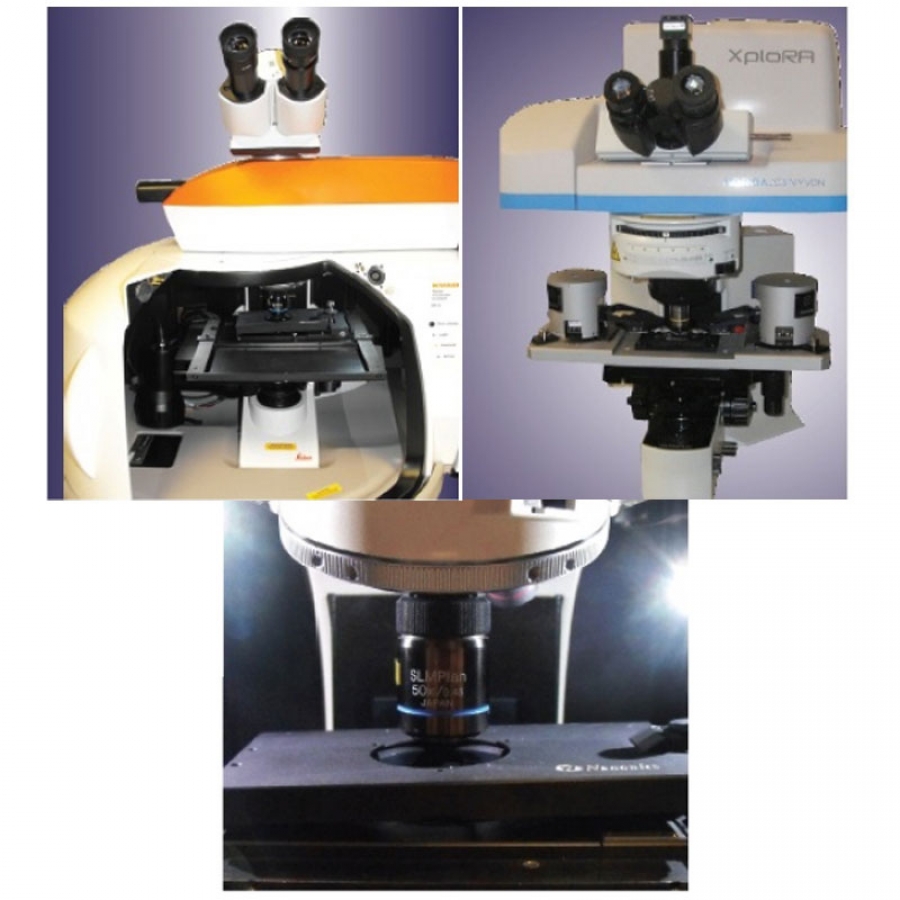
AFM Raman Direct Mounting:
Direct mounting of the AFM head on micro-Raman microscope under the Raman objective
| Renishaw Invia | HORIBA JY Explora |
 |
 |
| Thermo Scientific DXR | Bruker SENTERRA |
 |
 |
AFM Raman - Integration Package:
Integration Package allows for hard optical coupling of the Raman system with the AFM platform with complete isolation from noise mechanical noise sources. Clear optical axes are available from above and below for integration with upright, inverted and dual upright/inverted optical microscopes.
| Upright Integration Package | Dual Integration Package |
 |
 |
| Integration Package with Renishaw Invia | Integration Package with HORIBA Labram |
 |
 |
| Integration Package with CryoView System | Integration Package: Complete Separation |
 |
 |
Integration Package Advantages
- Flexible hard optical coupling to the Raman.
- Completely isolates the AFM from any noise from the Raman or lasers.
- The light is directly coupled from the Raman microscope to the AFM head and back to the spectrometer through infinity corrected optics.
- Direct illumination from above and below allows for the most effective coupling of the Raman laser to a TERS probe


