Graphene
Differentiating single, double, and multi-layers of Graphene

The Nanonics MultiView series (MV 1000, MV 2000, and MV 4000) provide complete hardware and software integration for the full suite of AFM and Raman characterization of all your materials including AFM, Raman, TERS, and NSOM characterization. AFM together with Raman based methods have become the method of choice for characterizing carbonaceous materials. For graphene, AFM-Raman imaging is especially useful for differentiating single, double, and multi-layers of graphene.
AFM-Raman of Graphene
A series of images of graphene flakes is shown. The first image (a) is an optical top-view of the graphene flake on silicon, collected with an upright optical microscope. Next is a 10um x 10um AFM height image (b) of the graphene flake showing 2 distinct areas. Figure (c) shows Raman spectra collected from the different areas, clearly differentiating the region of the single layer (red spectrum) and the double layer (blue spectrum.) Finally, a cross-sectional profile across one of these layers is shown in (d) showing a 6 angstrom step height, corresponding to the thickness of a single graphene flake.
")
")


In addition to Raman spectra being collected at individual points, AFM-Raman imaging enables the collection of a Raman image at a particular wavelength where the intensity of the Raman peak at that wavelength is mapped over the surface, simultaneously collected with topography from conventional AFM. In this way, an intensity map at the different Raman markers can be collected. For example, the 2676cm-1 band corresponding to the 2D band for the single layer or the 2700 cm-1 band corresponding to the double layer band can thus be mapped.
This has been done in the images below, where the Raman intensity has been overlaid on top of the 3D topography where red shows the highest Raman intensity and green is the lowest Raman intensity [blue coloring corresponds to region without any graphene]. On the left in (a) is the Raman intensity map of the 2676cm-1 single layer band, showing highest distribution of the single layer in the triangular red zone in the top half of the image. On the right is the AFM-Raman intensity map of the same area as (a) but now of the 2700cm-1 double layer band, showing the strongest signal in the top trapezoidal and bottom rectangular orange regions. Note that the single and double layer band regions are located in different areas of the surface and are easily identified using the Raman maps.


Tip-enhanced Raman spectroscopy (TERS) of graphene
Nanonics unique AFM-Raman integration allows for new horizons in graphene characterization with Tip Enhanced Raman Spectroscopy (TERS). In TERS, a metallized sharp tip is used to enhance the electric field signal at the tip’s end. Unique TERS probes are provided by Nanonics that contain a gold nanoparticle embedded in the surrounding glass; this kind of probe gives high dielectric contrast with a well-defined plasmonics resonance and without a Raman background. When combined with tuning fork (laser-free) feedback, this probe provides a completely free optical axis for top-viewing of opaque samples. Additionally, these probes provide considerable enhancement and so the use of these probes does not require a conductive substrate for Raman enhancement. Finally, the Multiview 2000 and Multiview 4000 offer both tip and sample scanning scanners, enabling quick and easy hotspot detection by tip positioning. The combined tip and sample scanning stage provides accurate positioning of the probe at the ideal location with respect to the focused laser spot and the sample can be scanned without losing the Raman hotspot position.
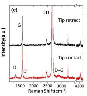
The data bellows shows an optical image on left of a TERS probe in top-view positioned on Graphene single and multi layers. The corresponding far-field (Black) and near-field enhanced (Red) spectra are shown on the right where the probe was in contact with the graphene single layer, resulting in the red TERS spectrum. The TERS spectrum clearly shows that only some of the Raman peaks are enhanced over the far-field spectrum, specifically the 1589cm-1 and 2677cm-1 peaks are enhanced. This shows that specific vibrational modes in the graphene are locally enhanced near the tip. Thus, the vertical resolution of the Raman data is significantly improved with TERS, which now enables distinction between the substrate and the upper layers.


Moving the tip to a different position on the surface as shown in the optical image below on the left, the interaction of the probe with the sample now reveals multilayer graphene, as revealed in the black (far-field) and red (TERS) spectrum on the right.
Raman Difference Spectroscopy
Nanonics has implemented into the Multiview 2000 and 4000 series a set of specialized AFM scanning protocols of Raman difference spectroscopy effectively discriminating between the near-field and far-field contribution of the scattered Raman signals. Such Raman difference protocols provide a selective enhancement of graphene single layer in-plane vibrational modes with lower effect of subsequent graphene layers. Moreover, such scanning protocols allow for maximizing Z polarization excitation even when using conventional Raman excitation with a Gaussian focused laser beam.
Below is an AFM image of graphene in i), where both far-field Raman (black), TERS (red) , and difference (green) spectra have been collected at a variety of spots on the surface. Spectra in ii) were collected at points (a) revealing a single layer of graphene. The spectra in iii), collected at point (b) reveal a double layer of graphene while the spectra in iv) collected at point (c) reveals 3-4 layers. This kind of difference mapping helps to identify the enhanced band only.

Other Multifunctional Graphene Imaging
Other important properties of graphene can be probed as well. Below, we show thermal and Kelvin probe images of graphene, collected simultaneously with height so that correlation with the topography is possible. AT bottom is a schematic showing the setup to probe the near-field photoconductivity of graphene.
1. Thermal-conductivity Imaging of Graphene

AFM (left) and Overlaid AFM/Thermal imaging (right) of graphene flakes performed with Nanonics Thermo-conductivity probe
2. AFM and Kelvin Probe Imaging of Graphene

AFM (left) and KPM (right) images of graphene transistor with opposite voltage bias
3. Near-field Photoconductivity of Graphene