Super User
3D FlatScan Scanning Stage
Support for MURI Funding Application
The deadline for the US Office of Naval Research MURI grant program is fast approaching. The Multidisciplinary University Research Initiatives (MURI) program is intended for "teams of researchers investigating high priority topics and opportunities that intersect more than one traditional technical discipline." With years of experience as leaders in multidisciplinary SPM research and development, Nanonics is uniquely positioned to assist you in your proposal.
Duration of Award: 3-5 years
Estimated Maximum Annual Sum: $1.5 million
Deadline for White Paper: July 17, 2017
Learn more about the MURI program
Download the Funding Opportunity Announcement
In the past, Nanonics has provided quotations, letters of support, and detailed technical consultations for researchers, employing a variety of our multidisciplinary SPM solutions. Nanonics specialists are here to support your research initiatives. Some examples:
-
Studying thermal transport with multiprobe SPM.
-
Understanding optomechanical dynamics with multiprobe SPM-based NSOM (Near Field Scanning Optical Microscopy).
-
Depositing materials in a controlled fashion for a variety of applications via nanolithography
Nanonics has designed its optically integrated multiprobe platforms to facilitate multidisciplinary research. The MURI program presents a unique opportunity to incorporate one of these high-end SPM systems into your research:

- Multiprobe SPM allows for studying and understanding a variety of nanoscale transport properties, e.g. thermal, mechanical, and optical.
- Access a variety of advanced SPM measurements: MFM, EFM, PFM, KPM.
- Full optical integration enables the addition of in situ measurements such as Raman, IR, THz, and fluorescent spectroscopy.

- This award-winning system upgrades the multiprobe platform to high-vacuum and low-temperature environments for studying samples in the most challenging of conditions.
- The CryoView is fully integrated with near-field and far-field optics, Raman, IR, THz, and fluorescent spectroscopy.
Contact a Nanonics Specialist today for support with YOUR proposal
Multi-Dimensional Metrology (MDM) Consortium Soon to Begin
 The Israeli chip consortium, MDM - Multi Dimensional Metrology, will begin operating in July 2017. following approval by the Innovation Authority.
The new consortium will deal with the development of measurement and process control technologies in the chip industry, based on data fusion from many sources. The consortium was established at the initiative of Applied Materials and the chairman of the consortium will be Yoram Uziel, director of technology at PDC, Applied Materials' Metrology Division. The State of Israel is expected to participate in approximately 66% of the consortium's budget via the Innovation Authority, for 3-5 years.
The new consortium will include leading companies in the field of process control, such as Bruker (which acquired Jordan Valley of Israel) and Nova; Dell EMC; Nanonics, leader in atomic microscopy measuring solutions; Nanomotion, which develops nanoscale conveyance systems; XWINSYS, which develops measurement equipment for critical final stages of the production line; and EL-MUL, from Nes Ziona, which manufactures detectors for the nanoscale industry. The academic side will include research groups from the Technion, Hebrew University, Tel Aviv University, the Weizmann Institute, Bar-Ilan University and Ben-Gurion University, which will also provide construction services for nanoscale structures.
Uziel defined the consortium’s area of focus as Multi-Dimensional Metrology, in order to express the idea that it is necessary today to integrate different sources of information from different measuring devices in order to overcome the limitations of accuracy, characterization, and resolution of new chips that will be released in the coming years. The industry today faces a number of new challenges. The chip minimization process, culminating in 5 nanometer geometry, and the transition to building 3D structures create difficult problems requiring a new type of technological response.
*Translation based on: http://chiportal.co.il/main-news/49-q/5452-mdm-concorcium-1306179
What are the Different NSOM Modes?
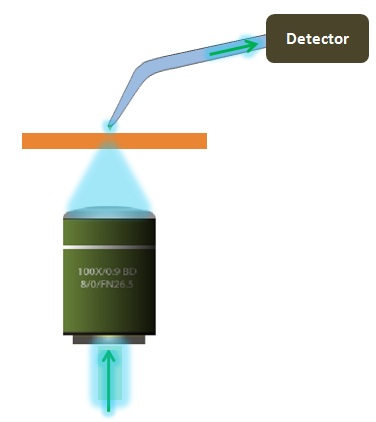
True Collection Mode

In this mode, light illuminates the sample and is then collected through the NSOM probe and measured by an optical detector; thus there is far field excitation with near-field collection as seen in the schematic (Far-field excitation from the top is also available). Note that the optical microscope objective is not used for feedback; the feedback is instead through the tip-probe interaction. The ability to scan the tip is important for collection mode so that the illumination point, either from above or below, is held fixed while the tip scans to collect the near-field signal.
NSOM transmission mode

In this mode, light is introduced through the optical fiber and collected by a detector underneath the sample as shown, allowing for NSOM imaging of transparent samples as shown in the schematic above. This is suitable for transparent or semi-transparent samples. Thus you can perform experiments that require near-field excitation and far-field collection.
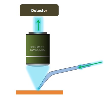
Reflection mode NSOM

In true reflection mode, light is introduced via the NSOM probe, and then collected by a detector above the probe as shown in the schematic below allowing for NSOM imaging of opaque samples. True Reflection mode NSOM requires the use of cantilevered probes with an extended tip such as the ones provided by Nanonics, as well as a free optical axis from above so that the probe does not obscure the optical path to the objective and then to the detector from above. Furthermore, true reflection mode NSOM requires a separation of the excitation and collection paths so that they don’t interfere with one another; designs where the excitation and collection follow the same path – as is the case for instrumentation that uses apertured Si NSOM probes or when the reflected light is collected from the sides as with straight fiber NSOM operated in shear force feedback - confound the NSOM measurement.


