

Super User
BEST CAFM Results in Comparative Study
BEST CAFM Results in Comparative Study
Unique Technology Avoids Photocurrent Artifacts
Review of Scientific Instruments 87(8), 083703
Yanfeng Ji, Fei Hui, Yuanyuan Shi, Vanessa Iglesias, David Lewis, Jiebin Niu, Shibing Long, Ming Liu, Alexander Hofer, Werner Frammelsberger, Guenther Benstetter, Andrew Scheuermann, Paul C. McIntyre and Mario Lanza
Photoactive materials play a crucial role in the development of energy storage devices, such as solar, electrochemical cells, and others. Conductive atomic force microscopy (CAFM) is a powerful tool for nanoscale electronic characterization of photoactive materials. It is well known that environmental light can alter the measurements when scanning photoactive samples. For this reason, measuring in a dark environment has been recognized as the standard CAFM process. However, as an optical feedback laser is necessary to acquire topography, the laser used in CAFM can also generate a high photocurrent, even without any bias between the conductive tip and the sample. While the laser-induced current signal perturbation is well known within the CAFM community, the observation of currents generated by the optical feedback laser in absence of bias is still not fully understood and has never been studied in depth.
For the first time, this paper studies and analyzes the photocurrent induced in the photoactive materials by the feedback laser. CAFM measurements were carried out on photoactive samples using six standard optical feedback AFMs of different manufacturers, as well as a Nanonics tuning-fork based feedback AFM (without using a laser).
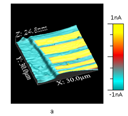
Seen in image: 3D Collage Map of topographic and current maps, collected on Ni electrode using the Nanonics MV4000 AFM without application of bias. The yellow regions were measured with illumination, in order to replicate a feedback laser, and high current is observed. In contrast, the blue regions were measured without any feedback laser, and thus in absolute darkness, and no current is observed.
"Direct Measurement of Nanoscale Lateral Carrier Diffusion: Toward Scanning Diffusion Microscopy"

Nanonics Visits Los Angeles!

Nanonics is pleased to be attending this year's APS March Meeting in Los Angeles!
We will be located at Booth #320 - Stop by to learn more about our leading AFM-Raman, TERS, and SECM solutions.
Be sure to catch, as well, Founder and CEO Professor Aaron Lewis's presentation on Thursday, March 8 at 10:24 AM:
Nanoprinting of Metallic Conductive Inks with Fountain Pen Nanolithography
See you in L.A.!
Nanonics is in Boston!


Nanonics is pleased to be attending this year's MRS Fall Meeting in Boston!
We will be located at Booth #817 - Stop by to learn more about our leading AFM-Raman and SECM solutions.
Be sure to catch, as well, our presentation on Tuesday, November 28 at 11:30 AM:
Nanoprinting of Metallic Conductive Inks with Fountain Pen Nanolithography
See you in Boston!
Model Home
Integrate SPM with Super Optical Resolution

Find the NSOM or AFM-Raman System that's Right for Your Research
Start exploring the possibilities today
Select One or Multiple Modes of Scanning Probe Microscopy
| NSOM |
AFM-Raman |
Bio-AFM |
 |
 |
 |

Join 100's of universities and corporations enjoying Nanonics SPM systems
SCIX2017
 Nanonics is thrilled to be represented by Flash-Photonics at this year's SCIX Conference. Come visit Booth 22 to learn more about AFM-Raman-TERS!
SECM SPM
SECM - Scanning Electrochemical Microscopy
Featuring in situ Raman Functionality

SECM is a tool which is used to measure processes mainly in the vicinity of a surface. This technique can be used for fuel cells research, surface reactivity of solid state materials, the elucidation of enzymatic activities and other biophysical investigations. These all call for the probe to be in the near vicinity of the analyzed surface and to be able to control its spatial orientation.
The AFM-SECM combination enables one to track the topography in real-time at a fixed working distance while electrochemical signals related to surface activity are collected at the probe. The ability to add on spectrochemical analysis enhances this technique and can set new horizons to electrochemical investigations. Monitoring the Raman signal at real time gives the ability to understand the dynamics of the chemical reactions occurring at a sub-micron resolution in the vicinity of the SECM probe.
Innovations in SECM
Nanonics systems provide unique liquid-based capabilities in scanning electrochemical microscopy (SECM) that now for the first time can be combined with other SPM methods such as AFM-Raman for chemical imaging together with the topographic and electrochemical current imaging. The Nanonics SECM capability incorporates Nanonics innovations in probe design, tip-sample feedback, and liquid cell design to enable new and revolutionary capabilities for the most advanced experiments.
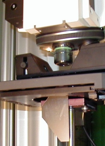
Probes
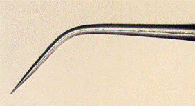
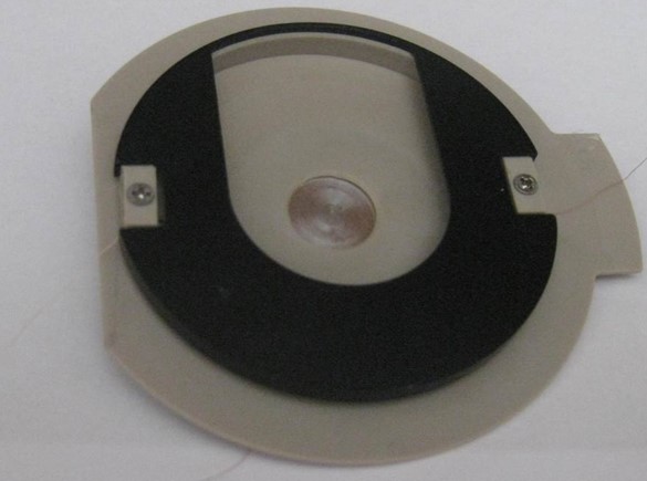
Nanonics manufactures custom SECM probes with a continuous nanowire of platinum embedded in glass. A side view is seen below on the left left while a top view is seen below on the right clearly showing the platinum wire and glass. In the top-view, the white spot in the middle is the wire; the black ring around it is the glass.

These custom probes provide simultaneous normal force sensing with full SECM functionality. Tip-sample feedback is maintained with the classic optical-based deflection method where a laser is reflected off the back end of this cantilever and directed towards a detector. Feedback can be maintained either via cantilever deflection or oscillation amplitude to keep the force, and hence tip-sample interaction, constant.
Liquid Cell/Environmental Chamber
Environmental Chamber
Nanonics provides a custom-designed liquid cell and environmental chamber to use in such measurements.

Liquid Cell - Exposed
Sample is placed in ring in the middle. Changeable wire electrodes are on the sides.
Liquid Cell - Partially Covered
SECM Cell that is partially covered to minimize evaporation.

Liquid Cell - Bottom
Contains back contact for applying voltage to the sample.

Liquid Cell
The electrochemical cell is specially designed to protect from spillage.
Raman Integration
Nanonics systems feature full integration capabilities for real-time SECM measurements with AFM force feedback and simultaneous Raman measurements. The Raman setup through the laser, spectrometer, and CCD camera are placed above the probe with the optically friendly scanner and probe. Fluid measurements are observed using the critically important water immersion objective.

Nanonics MV2000 SECM-Raman Integration
Especially effective with water immersion objectives from above on opaque materials.
(Pictured here with Renishaw InVia)
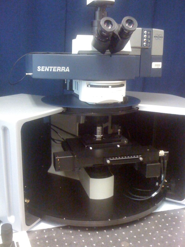
Nanonics MV2000 SECM-Raman Integration
(Pictured here with Bruker Senterra)

Nanonics MV4000 SECM-Raman Integration
Featuring multi-probe capabilities and unique Tuning Fork technology.
Nanonics MV15000 SECM-Raman Integration
Entry level with optical upgrade capability.
Case Study: Etching of Si Wafer with Au
SECM-Raman Application: Simultaneous SECM current and Raman imaging of copper during real-time etching
A silicon wafer with a thin layer of copper was used as the substrate for this electrochemical etching experiment. The SPM probe etched a small, ~4um hole within the copper layer, exposing the silicon substrate. Images of the substrate before (left) and after (right) the etching can be seen below with the etched point showing up as a dark spot in the right image.

The etching was monitored in real time with in situ Raman scattering where the Raman signature of silicon at 523 cm-1 was used to track the appearance of the silicon and thus progress of the etching process. A sample spectrum revealing the Si peak in the Raman spectrum is shown here:

Simultaneously, the current was monitored revealing a time delay between when the current was measured and when the exposed silicon was picked up the Raman spectra. This time delay was found to be dependent on the probe-substrate vertical distance.
Hot off the Press!

Nanonics is pleased to share with you the news of the recent publication of Conductive Atomic Force Microscopy: Applications in Nanomaterials, edited by Mario Lanza (Publisher: Wiley-VCH). The book includes a chapter entitled "Multiprobe Electrical Measurements without Optical Interference," written by Nanonics team members. This new publication will no doubt contribute greatly to the field of CAFM.
Photoconductivity-Photovoltaics
Photovoltaics
Photoconductivity Imaging with Super-Resolution

Reference: Mueller, T., Xia, F., Freitag, M., Tsang, J., & Avouris, P. (2009). Role of contacts in graphene transistors: A scanning photocurrent study. Physical Review B, 79(24), 245430.
The Growth of Solar Cell Energy & Photovoltaics
- Over the past decade, the solar cell energy industry has grown dramatically; photovoltaic research has emerged as a dynamic and ever-increasingly important field. Recent estimations indicate that total PV installations in the world have reached 300 GW – a 4000% increase since 2006!
(See: Kurtz, S., Haegel, N., Sinton, R., & Margolis, R. (2017). A new era for solar. Nature Photonics, 11(1), 3-5).
- The solar energy industry continues to push the bounds of the nanoscale and has been focused on increasing photovoltaic efficiency.
(See: Alharbi, F. H., & Kais, S. (2015). Theoretical limits of photovoltaics efficiency and possible improvements by intuitive approaches learned from photosynthesis and quantum coherence. Renewable and Sustainable Energy Reviews, 43, 1073-1089.)
- The innovative nanostructured solar cells that are being developed require advanced nanoscale instruments that can achieve accurate and high-resolution photoconductivity measurements.
- Now more than ever, the ability to obtain high resolution photoconductivity measurements is a critical element in the development of this growing solar cell industry. Such measurements are applicable to all photovoltaic materials, including:
| • Perovskite | • Ribbon-Si | • Si Thin-Film |
| • 2D Materials | • C-Si | • GaAs Thin-Film |
| • Graphene | • Mono-Si | • MLM |
| • MoS2 | • Poly-Si | • CdTe |
| • Expatial Si Wafers | • CIGS |
Limitations of Macroscopic Photoconductivity Techniques
Common photoconductivity techniques that employ standard Gaussian beam far-field optics are inherently limited:
1. Limited Resolution
The resolution of a lens focused beam gives at best 0.5micron resolution at 500nm illumination. Thus, such macroscopic photo-current methods study spatially averaged properties of the PV device and are ineffective for the study of nanostructured photovoltaic cells, nanoscale defects, grain boundaries, and thin film solar cells. Furthermore, the shape of a lens focused Gaussian beam makes it difficult to impossible to illuminate a sample next to an electrical contact.
2. No Structural Correlation
Most techniques do not include the capability to generate online nanometric sturctual correlation.
3. Out-of-Focus Background
Lenses focus below and above the sample plane and therefore feature an illumination background.
4. Sensitivity Reduction
Typically a reduction in sensitivity can be observed, due to regions illuminated that are not directly of interest.
5. Non-uniform Illumination
Scanning a beam over a sample with varying topography, or with some tilt in the mounting of the sample, leads to changes in light exposure from pixel to pixel thereby generating photovoltaic artifacts.
6. Partial Information
Standard macroscopic photoconductive measurements are unidimensional. They only offer photocurrent characterization, without any correlation to changes in other functional properties of a sample.
Top 5 Advantages of Nanonics Photoconductivity Near-Field Scanning Optical Microscopy
Nanonics systems for Near-field scanning photocurrent microscopy represent a fundamental paradigm shift in photoconductivity measurements, solving these limitations. Near field scanning probe microscopy (NSOM) allows for nanometric optical characterization with correlated sample morphology imaging. This innovative approach features 5 powerful advantages:
1. Super-Resolution
Imaging of light-induced current and voltage with previously unachievable; super-resolution down to 50nm
2. Photocurrent with Structural Correlation
Pixel by pixel correlation of device structure with photocurrent and photovoltage images
3. Uniform Illumination
Identical illumination at each pixel
4. Artifact-free
No optical background artifacts or noise
5. On-line Chemical Characterization
Readily correlate photoconductivity images with imaging of chemical structure
Example Case Study
Super-resolution Imaging of Photocurrent Induced in Graphene Transistor by Near-field Optical Excitation
Reference: Mueller, T., Xia, F., Freitag, M., Tsang, J., & Avouris, P. (2009). Role of contacts in graphene transistors: A scanning photocurrent study. Physical Review B, 79(24), 245430.
Customer Application:

•Super-resolution: Illuminating with an NSOM aperture down to 50nm in AFM feedback with the sample. Feedback is controlled with a tuning fork without any induced optical background.
[Read more: Review of Scientific Instruments 87, 083703 (2016)]
•Uniform Illumination: Using AFM feedback to maintain an exact distance from the surface for unvarying pixel by pixel illumination intensity with a top-hat intensity profile.
•Artifact-free: No background illumination either from the NSOM probe normal force tuning fork feedback or from variation in illumination intensity.
•Structural Correlation: Scanning the aperture with AFM feedback control to obtain simultaneously pixel by pixel structural correlation.
•On-line Chemical Characterization: A cantilevered NSOM probe that does not obscure the microscope's optical axis from above, allowing for spectral imaging on-line of Raman, fluorescence, etc.
•Multiprobe: Exclusive Nanonics multiprobe capabilities upgrades p-NSOM from one to four probes allowing for on-line Kelvin probe, electrical and thermal conductivity.
Exemplary Photoconductive Image of a Graphene Transistor Elucidating Effects of Metallic Contacts:
Additional Features
Enjoy Complete Optical Access
Nanonics SPM systems feature open optical access from above and below. This allows for the seamless integration of NSOM along with complementary macroscopic techniques for all optical geometries. With optical integration, you can obtain comprehensive characterization of PV devices. High resolution photoconductivity imaging can be readily correlated with all past measurement protocols including Raman and confocal microscopy.
Read more: Solar Energy Volume 153, 1 September 2017, Pages 134-141
Enable Advanced Applications with Mutliple SPM Probes
The exclusive Nanonics multiprobe system upgrades NSOM from one probe to two, three, or even four probes including probes for different SPM methods. Thus system with two NSOM probe provides subwavelength incoupling and outcoupling of light, which is most important for study photoconductive properties of thin films, 2D material-based photovoltaic cells and nano structural cells. Integration of NSOM probe with electrical, magnetic, KPFM and other SPM probes leads to simultaneous comprehensive characterization of photovoltaic devices, which is not possible with single probe systems. Each probe enables independent XYZ scanning together with sample scanning.
Read more: Nanoscale. 2017 May 25; 9 (20):6695-6702