Displaying items by tag: NSOM


"Characterization of the Photocurrents Generated by the Laser of Atomic Force Microscopes"

Review of Scientific Instruments 87(8), 083703.

Yanfeng Ji, Fei Hui, Yuanyuan Shi, Vanessa Iglesias, David Lewis, Jiebin Niu, Shibing Long, Ming Liu, Alexander Hofer, Werner Frammelsberger, Guenther Benstetter, Andrew Scheuermann, Paul C. McIntyre and Mario Lanza


Photoactive materials play a crucial role in the development of energy storage devices, such as solar, electrochemical cells, and others. Conductive atomic force microscopy (CAFM) is a powerful tool for nanoscale electronic characterization of photoactive materials. It is well known that environmental light can alter the measurements when scanning photoactive samples. For this reason, measuring in a dark environment has been recognized as the standard CAFM process. However, as an optical feedback laser is necessary to acquire topography, the laser used in CAFM can also generate a high photocurrent, even without any bias between the conductive tip and the sample. While the laser-induced current signal perturbation is well known within the CAFM community, the observation of currents generated by the optical feedback laser in absence of bias is still not fully understood and has never been studied in depth.

For the first time, this paper studies and analyzes the photocurrent induced in the photoactive materials by the feedback laser. CAFM measurements were carried out on photoactive samples using six standard optical feedback AFMs of different manufacturers, as well as a Nanonics tuning-fork based feedback AFM (without using a laser).

The results obtained show that the laser induces abundant parasitic photocurrent even without any bias in the other tested optical feedback AFMs. In contrast, the Nanonics MV4000 system based on Tuning Fork feedback does not induce parasitic photocurrent and thus provides a true current map in complete darkness.

3dcollage
3D Collage Map of topographic and current maps, collected on Ni electrode using the Nanonics MV4000 AFM without application of bias. The yellow regions were measured with illumination, in order to replicate a feedback laser, and high current is observed. In contrast, the blue regions were measured without any feedback laser, and thus in absolute darkness, and no current is observed.


Read the full abstract here 

Published in Publication Highlights
Tuesday, 08 March 2016 14:03

Scanning Polariton Interferometry

By combining the best of both worlds that photons and electrons have to offer, polaritons hold much promise for a variety of applications in optoelectronics and nanophotonics such as miniatiruzed circuits for improved information or energy transfer. Polaritons are hybrid or quasi particles that are made up of photons strongly coupled to an electric dipole. There are different kinds of polaritons such an electron-hole pair that form an exciton polariton, which is present in semiconductors, or electrons at a metal surface that create surface plasmon polaritons (SPPs). Exciton polaritons that are stable at ambient conditions are an active area of research interest. A particular group of semiconductor chalcogenide materials was recently identified to have the existence of polaritons under ambient conditions. However, these materials were previously investigated using far-field methods. These materials are important for their potential applications in information technology, bio-sensing and metamaterials.

In this work, a team of researchers led by Prof. Xu of University of Washington use a Nanonics MV 4000 operating in reflection NSOM to study waveguide polaritons in thin <300nm flakes of WSe2 at ambient conditions. Using this setup, they could directly excite and probe polariton modes by imaging their interference fringes in a method termed “scanning polariton interferometry” at different wavelengths to map out the entire polariton dispersion both above and below the excitation energy. In this study, the polaritons were observed to have a wavelength down to 300nm in WSe2 and propagate many microns below the excitation energy. The near-field illumination allowed for the first time direct excitation and real imaging of the exciton polariton without the need for complicated cavity fabrication. Furthermore, by tuning the excitation laser energy it was possible to map the entire polarity dispersion.


Contact us

To learn more about any Nanonics Systems feel free to contact us and speak to one of our experts.


Published in Publication Highlights

Patrice Genevet, Daniel Wintz, Antonio Ambrosio, Alan She, Romain Blanchardand Federico Capasso

Nature Nanotechnology PUBLISHED ONLINE: 6 JULY 2015 | DOI: 10.1038/NNANO.2015.137

When a charged particle travels faster than the phase speed of light in a medium, a photonic shock wave called Cherenkov radiation is emitted. This electromagnetic shock wave is emitted as a cone in the three spatial dimensions. In this paper it was shown that a two dimensional analogue of Cherenkov radiation can be created to control and steer plasmons in one-dimensional metamaterials.

A one-dimensional metasuface was fabricated for the experiment, which consisted of an array of slits in different directions etched in the thin metal film. S-polarized light illuminates the metasurface in far-field and creates running waves of polarization (RWP). The RWP can be understood as a series of dipoles oriented normally to the slit axis
with different phases generated along the metasurface. These dipoles interact with the local distribution of free electrons on the metal surface and radiate SPP waves along the metal–dielectric surface. The RWP propagation speed is always larger than the SPP phase velocity. SEM image of nano- array structure

EM image of nano- array structure

Thus two-dimensional Cherenkov radiation is generated in the metasurface.
Moreover both experimental and theoretical analyses have showed that the direction of the Cherenkov radiation depends on the

angle and spin of the incident polarized light. Thus the propagation direction of the Cherenkov radiation can be controlled and steered by either one of these parameters.The experimental results show that that the direction of the SPP wakes depends on the angle and spin of the incident light. Thus the steering of the SPPs wakes can be achieved by variation of either one these parameters. The propagation direction of the two- dimensional Cherenkov radiation can be steered from forward to backward.

The experimental results are in the good agreement with the theoretical simulation.

The obtained results are very important step toward in understanding of the SPPs wakes propagation. The ability to control and manipulate of the SPPs propagation direction opens new horizons in development of novel plasmonic devices such as plasmonic phase modulators, plasmonic couplers, plasmonic holograms and beam-steering devices.


Experimental results. Forward Cherenkov SPP wakes (left), backward Cherenkov SPP wakes (right). Θ is angle of circular polarized incident light; σ+ and σ- are spin of the polarization, ϒ angle of Cherenkov SPP wakes propagation 


Experimental Setup:

The experimental analysis of the SPPs wake propagation was performed with a Nanonics Multiprobe MV 4000 near-field optical microscope in collection mode (with the NSOM probe collecting the light into a detector).  The MV 4000 allowed for such an experiment as a result of the following advantages:

  • Free optical access of the NSOM head from the both the top and the bottom. Allowing for direct illumination of the sample from below and easy visualization of the tip and sample from above.
  • Tip scanning allowing NSOM mapping of the SPP independent to the illumination and without moving the sample.
  • Topographic and near-field optical data are acquired simultaneously by scanning with Nanonics cantilevered NSOM probe.
  • Tuning fork (TF) feedback allows for no optical AFM feedback and no optical interference with the measurement
  • It is important to note that Apertured NSOM is important for such an experiment as an apertureless NSOM configuration would require laser illumination at the tip which can interferes with the Cherenkov radiation and lead to optical artifacts.
Published in Publication Highlights
Monday, 08 February 2016 14:05

Photonics and Silicon Photonics


Published in Learn NSOM
Wednesday, 29 July 2015 14:32

Plasmonics


Plasmonics

Case Study: Cherenkov SPPs


Patrice Genevet, Daniel Wintz, Antonio Ambrosio, Alan She, Romain Blanchardand Federico Capasso

Nature Nanotechnology

PUBLISHED ONLINE: 6 JULY 2015 | DOI: 10.1038/NNANO.2015.137

When a charged particle travels faster than the phase speed of light in a medium, a photonic shock wave called Cherenkov radiation is emitted. This electromagnetic shock wave is emitted as a cone in the three spatial dimensions. In this paper it was shown that a two dimensional analogue of Cherenkov radiation can be created to control and steer plasmons in one-dimensional metamaterials.

A one-dimensional metasuface was fabricated for the experiment, which consisted of an array of slits in different directions etched in the thin metal film. S-polarized light illuminates the metasurface in far-field and creates running waves of polarization (RWP). The RWP can be understood as a series of dipoles oriented normally to the slit axis
with different phases generated along the metasurface. These dipoles interact with the local distribution of free electrons on the metal surface and radiate SPP waves along the metal–dielectric surface. The RWP propagation speed is always larger than the SPP phase velocity. SEM image of nano- array structure

EM image of nano- array structure

Thus two-dimensional Cherenkov radiation is generated in the metasurface.
Moreover both experimental and theoretical analyses have showed that the direction of the Cherenkov radiation depends on the

angle and spin of the incident polarized light. Thus the propagation direction of the Cherenkov radiation can be controlled and steered by either one of these parameters.The experimental results show that that the direction of the SPP wakes depends on the angle and spin of the incident light. Thus the steering of the SPPs wakes can be achieved by variation of either one these parameters. The propagation direction of the two- dimensional Cherenkov radiation can be steered from forward to backward.

The experimental results are in the good agreement with the theoretical simulation.

The obtained results are very important step toward in understanding of the SPPs wakes propagation. The ability to control and manipulate of the SPPs propagation direction opens new horizons in development of novel plasmonic devices such as plasmonic phase modulators, plasmonic couplers, plasmonic holograms and beam-steering devices.


Experimental results. Forward Cherenkov SPP wakes (left), backward Cherenkov SPP wakes (right). Θ is angle of circular polarized incident light; σ+ and σ- are spin of the polarization, ϒ angle of Cherenkov SPP wakes propagation 


Experimental Setup:

The experimental analysis of the SPPs wake propagation was performed with a Nanonics Multiprobe MV 4000 near-field optical microscope in collection mode (with the NSOM probe collecting the light into a detector).  The MV 4000 allowed for such an experiment as a result of the following advantages:

  • Free optical access of the NSOM head from the both the top and the bottom. Allowing for direct illumination of the sample from below and easy visualization of the tip and sample from above.
  • Tip scanning allowing NSOM mapping of the SPP independent to the illumination and without moving the sample.
  • Topographic and near-field optical data are acquired simultaneously by scanning with Nanonics cantilevered NSOM probe.
  • Tuning fork (TF) feedback allows for no optical AFM feedback and no optical interference with the measurement
  • It is important to note that Apertured NSOM is important for such an experiment as an apertureless NSOM configuration would require laser illumination at the tip which can interferes with the Cherenkov radiation and lead to optical artifacts.
Published in Application Notes

Graphene Transistor


A unique protocol of near-field excitation for generating photocurrent with strong impact in solar cell applications is demonstrated here. A near-field scanning optical microscope has been used to locally induce photocurrent in a graphene transistor with high spatial resolution. By analyzing the spatially resolved photoresponse, it is shown that in the n-type conduction regime a p-n-p structure forms along the graphene device due to the doping of the graphene by the metal contacts.

The left picture shows the SEM image of a graphene transistor and the electrical setup for PC measurements. On the right seven PC images taken at gate biases between -60 and +100 V are shown. The dashed lines indicate the edges of the source and drain electrodes. The two scale bars on the bottom of the very right image are both 1 nm long.

Schematic illustration of the experimental setup and sample structure.


Mueller et al. PHYSICAL REVIEW B 79, 245430 2009

Published in Publication Highlights
Sunday, 08 February 2015 14:18

Nanoscale texture of secondary cell walls

Plant dry matter or lignocellulosic biomass is a feedstock of bioenergy, biofuel production and novel biomaterials. Understanding the cell wall structure is important for effective utilization of the lignocellulosic biomass.

Structure, chemistry and mechanics of the polymer assembly of the secondary cell walls have been studied for decades on the macrolevel. However, characterization of the chemical components of the cell walls on the nanolevel are still unknown due to the limitation in spatial resolution of spectral techniques such as FTIR and Raman, which are used  for chemical analysis.  

Most secondary cell walls of xylem cells are made up of three dominating polymers: cellulose, lignin and hemicelluloses. Cellulose fibrils with diameter 3-4 nm are arranged in larger agglomerates with size of 20-25 nm and are embedded in a matrix consisting of lignin and hemicelluloses. Different theoretical models of special arrangement of the polymers in the cell walls have been suggested. Most of these models are based on the SEM or AFM study but not on the chemical information.

In this work, a Nanonics MultiView 2000 with Near-field Scanning Optical Microscopy (NSOM) was used  for the first time to study the photo-optical and thus chemical properties of cell walls at the nanoscale. This technique enables scientists to overcome the optical diffraction limit and to reach the spatial resolution of 50nm (limited to size of the NSOM aperture)

The cell walls of three different plants-beeches (hard-wood), spruce (soft wood) and bamboo (grass) were studied with NSOM.


Since the samples are semi-transparent, the NSOM measurements were conducted in reflection mode. In this mode the light coming out from the probe aperture interacts with the sample, is reflected and then collected from the top with an optical objective of an upright microscope. The NSOM measurements were performed with a Nanonics MultiView 2000 and Nanonics cantilevered NSOM probes. The MV-2000 scanning head has a completely open optical axis from the top and from the bottom and can be easily integrated with almost any kind of optical microscopes. MV-2000 together with cantilevered NSOM probes, which have extended tip and special geometry, enable true reflection NSOM measurements.

Three images were acquired simultaneously: height, phase and NSOM. The obtained NSOM images showed curls- like structures with dimensions about 125 nm and more, which are not seen in the height and phase images. It is most likely that lignin contributes a stronger NSOM signal than cellulose and hemicelluloses due to its interaction with light (autofluorescence and resonance effect). NSOM results obtained on the three different plants species (hard wood, soft wood and grasses) point to the universal principle of the special cellulose and lignin assembly in secondary cell walls. For the first time, NSOM images provide sub diffraction limited chemical information about the spatial distribution of the secondary cell wall components. This contributes to the understanding of the cell wall structure and its enzymatic degradation for energy conversion from ligninocellulosic raw material in general.  

Published:  Keplinger et al. Plant Methods 2014, 10:1 

Click here for more information on this Nanonics MV 2000 system

Published in Publication Highlights
Wednesday, 04 February 2015 00:36

Multiprobe apertureless NSOM

Unique apertured and apertureless NSOM protocols with low background


MultiProbe Apertureless NSOM ANSOM 

Link to pdf version of app note

 In standard approaches to apertureless NSOM (ANSOM) the probe is simply a modulated scatterer with gross far-field optical illumination using elements such as lenses or mirrors, which cause large spot sizes of radiation around the scattering probe. 

It has been very chellenging to develop ways to reduce the artifacts that arise from the background that is created by these far-field optical elements; this background can interfere with the desired signal from the nanometric tip of an atomic force sensor capturing the near-field surface component in a large far-field radiation background.

The MultiView 4000 with its unique multiprobe capability enables the reduction of both the optical and mechanical background and thus increase the overall S/N.

One probe can be used as a limited illumination spot onto a second scattering probe.  This both reduces the optical background and generates the correct k vectors to excite the scattering probe.  In addition, since the feedback employs tuning forks, the scattering probe can be kept with an oscillation amplitude of 1 nm.  This has been shown to be critical due to the fact that the probe tip has to be modulated close to the surface without a jump to contact and without variation in z which adds additional background to the signal from mechanical sources.  Furthermore, the rigid tuning fork frequency significantly enhances heterodyne and homodyne lock-in detection schemes to further reduce background.

This scheme diagrammatically describes the two probe configuration where the illuminating probe excites the scattering probe and this probe can even be a single gold nanoparticle with high scattering contrast at the exposed tip of the AFM probe for increased signal from the very tip of the probe.  These probes have been developed by Nanonics for Tip Enhanced Raman Spectroscopy
   

Near-Field Plasmon Excitation & Apertureless Scattering and Collection  Apertureless NSOM ANSOM

A Multiview 4000 with a two Probe SPM setup has been used for effective localized illumination of a plasmonic structure with an apertured NSOM probe which produces all k-vectors, and so it is most efficient for such plasmonic propagation. The propagating plasmons are scattered and then collected with a second probe, which has a very low dielectric constant and minimal perturbation of the plasmonic propagation

Two Probe Setup Scheme: An apertured probe to produce an evanescent field with a spectrum of k vectors to effectively excite SPP (Left Probe). Right probe is a very low dielectric contrast, highly exposed, non-interfering scanning and work in Photon Tunneling mode to scatter SPP and directly collect the photons produced by such scattering MV4000 picture of two probes in close nanometric proximity. MV4000 provides flexible probe and sample piezo scanning stages for fine and coarse probe positioning and scanning. The image above shows two probe attached to Tuning Forks for the ultimate in AFM force sensitivity. A microscope picture (100x objective) top view shows two tips of apertured (Left) NSOM fiber probe providing 532nm near-field illumination and an Apertureless NSOM probe (Right). Surface plasmons are generated on top of an Au strip and scattered by the scanning ANSOM tip.


Left: AFM Height image of the Au strip performed with the ANSOM scanning tip. The circle at the bottom shows the effect of the illumination apertured tip when scanning in its close proximity. Middle: ANSOM image performed with the scanning tip.  Rich contrast is seen by the apertureless probe doing the AFM and ANSOM imaging. Right: 3D ANSOM image shows sustained plasmon propagation and then rapid decay

 Apertureless Probes  

Standard probes that need to be used in order to effectively scatter the plasmonic signal have significant perturbation on the plasmonic propagation because of the need to use probes with high dielectric constant to obtain effective signal to noise in such scattering experiments. 
Nanonics exclusively provides Apertureless probes of glass with plasmonic or Non-Plasmonic Scattering Particles.  Nanonics ANSOM probes are low dielectric constant, provide non-interfering scanning, highly exposed and work in Photon Tunneling Mode to scatter SPP. For such plasmonic probes, glass provides for high dielectric contrast for exceptional antenna effects at the tip of the probe.  Such probes can be provided with a nanoparticle as small as 10 nm or simple 5nm diameter glass probes.

Apertureless IR NSOM, nanoIR  

In the IR ANSOM regime standard far-field optical elements give large spot sizes of microns to tens of microns which seriously compromise the nature of the signal detected by the nanometric tip of an atomic force sensor.  Applying a Dual Probe system allows for ultra low background with minimal spot illumination size through an infrared fiber probe, which is nanometrically held in close proximity using the dual probe geometry to a scattering low dielectric glass probe or a single  gold nanoparticle probe or a silicon exposed tip probe.  Such a tip is generally modulated in close proximity to a surface in order to delineate the near-field interactions.

NanoIR Probe: Unique methods for IR illumination with a 100 nm point heat source for broad band IR irradiation of a scattering probe tip using multiple probe capabilities and with subsequent interfero-metric IR spectral resolution.  Overcome tens of micron spot sizes with lens based IR optical illumination.

Nanonics MultiProbe Apertureless NSOM: 

  • Multiprobe systems are singularly capable of exceptional apertureless and scattering NSOM imaging.

  • Ideal Apertureless solution with minimum stray light & maximum plasmonic excitation

  • MultiProbe ANSOM appears to have significant potential to reduce background and maximizing signal at the highest resolution

Published in Application Notes

Nanocoax ( metal- dielectric- metal) structures are potential devices for nanoscale photonics systems such as polarization- preserving optical waveguides for optical communication. It is very important to know the propagating properties of such structure for different excitation wavelengths.

NSOM is the best tool for study of such plasmonic nanodevices since the nSOM measurement is not diffraction-limited, and it provides both topographic and optical data with high resolution.

A Nanonics MV-4000 system was used for the AFM/NSOM measurements. This system enables scanning with probe as well as with the sample. The tip scanning capability is absolutely necessary for the study of objects requiring any form of constant optical alignment. The feedback in this system is based on the tuning fork, hence there no interference between the beam bounce laser and the light propagating through the sample.

The sample with the nanocoax array was specially prepared. The sample was illuminated from the bottom with different light sources: 473 nm, 532 nm, 660nm 850 nm. The light was transmitted through the nanocoax structures, collected via cantilevered NSOM probe (aperture diameter 100 nm), and detected with an avalanche photodiode.

Experimental results together with numerical calculations showed that the propagated modes have a different nature depending on the excitation wavelength, i.e, plasmonic TE11 and TE21 modes in the near infrared and photonic TE31, TE41 and TM11 modes in the visible. Far field transmission out of the nanocoaxes is dominated by the superposition of Fabry-Perot cavity modes resonating in the structures, consistent with theory. 

In summary, propagation of the plasmonic and photonic modes in nanocoax structures was experimentally observed for the first time in this work.

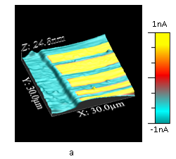
Fig. 1    NSOM-measured (a - d) and calculated (f - i) images of the propagated modes in the nanocoax structure. The wavelengths were 850 nm (a, f), 660 nm (b, g), 532 nm (c, h) and 473 nm (d, i). In all cases, the polarization is in the vertical direction, the scale bars represent 200 nm and circles represent the inner and outer radii of the coax annuli. (e) Three-dimensional representation of the nanocoax topography (lower, via AFM) and the corresponding near-field intensity (upper) for 532 nm wavelength. 

Published:  Optics Express June 16, 2014 Vol 22, No. 12

Click here for more information on the Nanonics MultiView 4000 system

Published in Publication Highlights

Near-field excitation and near-field detection of propagating surface plasmon polaritons (SPPs) on Au waveguide structures  

MultiProbe Apertured NSOM Plasmonic Charactarization

Near-field excitation and near-field detection of propagating surface plasmon polaritons on Au waveguide structures has been perfomed with Nanonics Multiview 4000 Dual Probe system

 Schematic of the MV4000 experimental setup for near-field excitation and near-field collection of SPP on gold waveguide structure (SEM shown inset)   AFM and NSOM 3D images of the Au Waveguide and the SPP distribution. The arrow shows the position of the illumination probe. The NSOM image shows exponential SPP decay with a propagation length of 550nm

Published: Appl. Phys. Lett. 94, 243118 (2009)

Click here for more information on the Nanonics Multiview 4000 system

Published in Publication Highlights
Page 1 of 2