
Displaying items by tag: MV4000
Characterization of the Photocurrents Generated by the Laser of Atomic Force Microscopes
"Characterization of the Photocurrents Generated by the Laser of Atomic Force Microscopes"
Review of Scientific Instruments 87(8), 083703.
Yanfeng Ji, Fei Hui, Yuanyuan Shi, Vanessa Iglesias, David Lewis, Jiebin Niu, Shibing Long, Ming Liu, Alexander Hofer, Werner Frammelsberger, Guenther Benstetter, Andrew Scheuermann, Paul C. McIntyre and Mario Lanza
Photoactive materials play a crucial role in the development of energy storage devices, such as solar, electrochemical cells, and others. Conductive atomic force microscopy (CAFM) is a powerful tool for nanoscale electronic characterization of photoactive materials. It is well known that environmental light can alter the measurements when scanning photoactive samples. For this reason, measuring in a dark environment has been recognized as the standard CAFM process. However, as an optical feedback laser is necessary to acquire topography, the laser used in CAFM can also generate a high photocurrent, even without any bias between the conductive tip and the sample. While the laser-induced current signal perturbation is well known within the CAFM community, the observation of currents generated by the optical feedback laser in absence of bias is still not fully understood and has never been studied in depth.
For the first time, this paper studies and analyzes the photocurrent induced in the photoactive materials by the feedback laser. CAFM measurements were carried out on photoactive samples using six standard optical feedback AFMs of different manufacturers, as well as a Nanonics tuning-fork based feedback AFM (without using a laser).
The results obtained show that the laser induces abundant parasitic photocurrent even without any bias in the other tested optical feedback AFMs. In contrast, the Nanonics MV4000 system based on Tuning Fork feedback does not induce parasitic photocurrent and thus provides a true current map in complete darkness.
Read the full abstract here
Scanning Polariton Interferometry
 By combining the best of both worlds that photons and electrons have to offer, polaritons hold much promise for a variety of applications in optoelectronics and nanophotonics such as miniatiruzed circuits for improved information or energy transfer. Polaritons are hybrid or quasi particles that are made up of photons strongly coupled to an electric dipole. There are different kinds of polaritons such an electron-hole pair that form an exciton polariton, which is present in semiconductors, or electrons at a metal surface that create surface plasmon polaritons (SPPs). Exciton polaritons that are stable at ambient conditions are an active area of research interest. A particular group of semiconductor chalcogenide materials was recently identified to have the existence of polaritons under ambient conditions. However, these materials were previously investigated using far-field methods. These materials are important for their potential applications in information technology, bio-sensing and metamaterials.
In this work, a team of researchers led by Prof. Xu of University of Washington use a Nanonics MV 4000 operating in reflection NSOM to study waveguide polaritons in thin <300nm flakes of WSe2 at ambient conditions. Using this setup, they could directly excite and probe polariton modes by imaging their interference fringes in a method termed “scanning polariton interferometry” at different wavelengths to map out the entire polariton dispersion both above and below the excitation energy. In this study, the polaritons were observed to have a wavelength down to 300nm in WSe2 and propagate many microns below the excitation energy. The near-field illumination allowed for the first time direct excitation and real imaging of the exciton polariton without the need for complicated cavity fabrication. Furthermore, by tuning the excitation laser energy it was possible to map the entire polarity dispersion.
To learn more about any Nanonics Systems feel free to contact us and speak to one of our experts. |

Controlled steering of Cherenkov surface plasmon wakes with a one-dimensional metamaterial
Patrice Genevet, Daniel Wintz, Antonio Ambrosio, Alan She, Romain Blanchardand Federico Capasso
Nature Nanotechnology PUBLISHED ONLINE: 6 JULY 2015 | DOI: 10.1038/NNANO.2015.137
When a charged particle travels faster than the phase speed of light in a medium, a photonic shock wave called Cherenkov radiation is emitted. This electromagnetic shock wave is emitted as a cone in the three spatial dimensions. In this paper it was shown that a two dimensional analogue of Cherenkov radiation can be created to control and steer plasmons in one-dimensional metamaterials.
| A one-dimensional metasuface was fabricated for the experiment, which consisted of an array of slits in different directions etched in the thin metal film. S-polarized light illuminates the metasurface in far-field and creates running waves of polarization (RWP). The RWP can be understood as a series of dipoles oriented normally to the slit axis | |
| with different phases generated along the metasurface. These dipoles interact with the local distribution of free electrons on the metal surface and radiate SPP waves along the metal–dielectric surface. The RWP propagation speed is always larger than the SPP phase velocity. | EM image of nano- array structure |
| Thus two-dimensional Cherenkov radiation is generated in the metasurface. | |
| Moreover both experimental and theoretical analyses have showed that the direction of the Cherenkov radiation depends on the | |
|
angle and spin of the incident polarized light. Thus the propagation direction of the Cherenkov radiation can be controlled and steered by either one of these parameters.The experimental results show that that the direction of the SPP wakes depends on the angle and spin of the incident light. Thus the steering of the SPPs wakes can be achieved by variation of either one these parameters. The propagation direction of the two- dimensional Cherenkov radiation can be steered from forward to backward. The experimental results are in the good agreement with the theoretical simulation. The obtained results are very important step toward in understanding of the SPPs wakes propagation. The ability to control and manipulate of the SPPs propagation direction opens new horizons in development of novel plasmonic devices such as plasmonic phase modulators, plasmonic couplers, plasmonic holograms and beam-steering devices. |
 Experimental results. Forward Cherenkov SPP wakes (left), backward Cherenkov SPP wakes (right). Θ is angle of circular polarized incident light; σ+ and σ- are spin of the polarization, ϒ angle of Cherenkov SPP wakes propagation |
Experimental Setup:
The experimental analysis of the SPPs wake propagation was performed with a Nanonics Multiprobe MV 4000 near-field optical microscope in collection mode (with the NSOM probe collecting the light into a detector). The MV 4000 allowed for such an experiment as a result of the following advantages:
- Free optical access of the NSOM head from the both the top and the bottom. Allowing for direct illumination of the sample from below and easy visualization of the tip and sample from above.
- Tip scanning allowing NSOM mapping of the SPP independent to the illumination and without moving the sample.
- Topographic and near-field optical data are acquired simultaneously by scanning with Nanonics cantilevered NSOM probe.
- Tuning fork (TF) feedback allows for no optical AFM feedback and no optical interference with the measurement
- It is important to note that Apertured NSOM is important for such an experiment as an apertureless NSOM configuration would require laser illumination at the tip which can interferes with the Cherenkov radiation and lead to optical artifacts.
Localized Charge Transfer Process
Localized Charge Transfer Process and Surface Band
Bending in Methane Sensing by GaN Nanowires
Avinash Patsha, Prasana Kumar Sahoo, Sankarakumar Amirthapandian, Arun K.
Prasad, Arindam Das, Ashok Kumar Tyagi, Monica Alonso Cotta, and Sandip Dhara
J. Phys. Chem. C,27 Aug 2015
Unique optical, electrical and mechanical properties of semiconductor nanowires make them very attractive as building blocks for novel LEDs, transistors, chemical and biological sensors. Recently was found that GaN nanowires are sensitive to methane CH4 gas and can be used for fabrication of the advanced gas sensor. The detection of potential greenhouse gas methane CH4 is extremely demanding in environmental safety.
Study of the sensing mechanism in the GaN nanowires is very important for improvement of the gas detectors performances. Recent studies were dedicated to the global characterization of the sensing processes in nanowires ensemble based gas detectors. The underlying physiochemical mechanism of gas detector operation is absorption of the gaseous molecules and subsequent transfer and transport of charge on semiconductor surface. However, detectors based on the nanostructures show more complex behavior due to the high surface- to-volume ratio. Thermally stable and chemically inert semiconducting surfaces such as GaN and AlGaN utilize the Schottky junction with metal or heterojunctions with other semiconducting surfaces as active sites in charge transfer and thus in sensing process. However, the sensitive properties of these semiconductors nanowires in III-nitrides group are strongly influenced by the present of intrinsic or extrinsic defects such as oxygen impurities.
Most studies of the GaN nanowire based detectors characterize them globally. This paper for the first time reports about the study of the localized charge transfer and thus sensing mechanism in single GaN nanowire. Role of the surface defects formed by the oxygen impurities in the single nanowire was also investigated. This localized characterization of the single nanowire was possible due to Nanonics Multiprobe Scanning Microscope. This multiprobe SPM enables to use two independent cantilevered probes (up to four probes) for different SPM methods. Study of the localized charge transfer in the single nanowire in result of gaseous molecular adsorption requires application of two probes: one for local gas delivery and the second one to probe the contact potential difference (CPD). During the sensing process, the chemisorbed molecules on the semiconductor surface induce bending of the energy band near the semiconductor surface, which cause changes in CPD. This surface band bending (SBB) can be studied as a function of CPD distribution, which is probed by scanning Kelvin probe microscopy. SBB is also strongly influenced by intrinsic and extrinsic defects, surface states, adsorbed gas or chemical molecules, temperature.
Experimental setup: Four GaN nanowires samples with different oxygen concentrations: 105 ppm, 103 ppm, 102 ppm and <2pmm were synthesized. Presence of N and O in the samples was identified with EELS method.
Multiprobe system with cantilevered fountain nano-pipette (opening diameter 200 nm) for localized gas delivery and conductive probe for Kelvin probe microscopy were used. The probes were moved close to each other and approached to the single nanowire with AFM feedback. Thus GaN single nanowire was exposed locally to the methane while the CPD and topography were acquired with conductive Kelvin probe. CPD was studied as a function of the nanowire diameters and oxygen impurity concentration.
The CPD showed a deceasing in the SBB value with an increasing in diameter. The increasing of the oxygen concentration in the nanowire causes the decreasing of the SBB value as well.
The observed variations in SBB value, depletion width, and surface charge density during nanowires exposed to methane confirmed the occurrence of gas adsorption and change transfer process in GaN nanowires. A localized charge transfer process, involving defect complex in nanowires is attributed in controlling the global sensing behavior of the oxygen rich GaN nanowire ensemble.
Nonradiating Anapole Modes in Dielectric Nanoparticles
Physicists have found a new way to confine electromagnetic energy without it leaking using nonradiating anapole modes. Nonradiating electromagnetic sources continue to be of interest as a model for stable atoms and to understand why orbiting electrons do not radiate, and have potential applications for combatting energy losses and explaining dark matter. The radiationless anapole mode is achieved by dividing the current between two different components, a conventional electrical dipole and a toroidal dipole. The radiation or far-field scattering is cancelled out if these two configurations are out of phase rendering the feature invisible.
 Scientists Miroshnickenko and colleagues tested this theory with near-field characterization of single silicon nanodisks of 50nm height and 200nm-400nm diameter, which were made effectively invisible by cancelling the disc’s scattering of visible light. The existence of an optical anapole mode in these nanodisks was investigated in both the far field and near field; the near-field characterization was critical for the device becomes invisible and thus undetectible in the far-field at the mode's excitation. A spectral dip in the far-field spectrum was observed corresponding to the dark anapole mode excitation, while near-field distribution of the disks was mapped at different wavelengths. The image on the right shows (a) far-field scattering spectra and (b) near field map for a 310nm diameter disk, where the far-field spectrum dip is most pronounced at 620nm.
Near field characterization was done with a CryoView MP that provides optical access from the top and from the bottom. It enables easy integration with all conventional optical microscopes for near field measurements in transmission, true reflection and collection modes. Both tip scanning and sample scanning are possible in the same scanning head which is especially important for the optical measurements described in this paper. The sample was illuminated in the far field using a supercontinuum source while transmitted light was collected in near field with a Nanonics cantilevered NSOM probe. with aperture diameter 50 nm during tip scanning. The Nanonics MV 4000 scanning head together with unique Nanonics cantilevered NSOM probes are the best tools for optical characterization of nanodevices in the near field with nanometric resolution.
Published: NATURE COMMUNICATIONS 2015
Click here for more information on the CryoView MP system
Plasmonics
Plasmonics
Case Study: Cherenkov SPPs
Patrice Genevet, Daniel Wintz, Antonio Ambrosio, Alan She, Romain Blanchardand Federico Capasso
Nature Nanotechnology
PUBLISHED ONLINE: 6 JULY 2015 | DOI: 10.1038/NNANO.2015.137
When a charged particle travels faster than the phase speed of light in a medium, a photonic shock wave called Cherenkov radiation is emitted. This electromagnetic shock wave is emitted as a cone in the three spatial dimensions. In this paper it was shown that a two dimensional analogue of Cherenkov radiation can be created to control and steer plasmons in one-dimensional metamaterials.
| A one-dimensional metasuface was fabricated for the experiment, which consisted of an array of slits in different directions etched in the thin metal film. S-polarized light illuminates the metasurface in far-field and creates running waves of polarization (RWP). The RWP can be understood as a series of dipoles oriented normally to the slit axis | |
| with different phases generated along the metasurface. These dipoles interact with the local distribution of free electrons on the metal surface and radiate SPP waves along the metal–dielectric surface. The RWP propagation speed is always larger than the SPP phase velocity. | EM image of nano- array structure |
| Thus two-dimensional Cherenkov radiation is generated in the metasurface. | |
| Moreover both experimental and theoretical analyses have showed that the direction of the Cherenkov radiation depends on the | |
|
angle and spin of the incident polarized light. Thus the propagation direction of the Cherenkov radiation can be controlled and steered by either one of these parameters.The experimental results show that that the direction of the SPP wakes depends on the angle and spin of the incident light. Thus the steering of the SPPs wakes can be achieved by variation of either one these parameters. The propagation direction of the two- dimensional Cherenkov radiation can be steered from forward to backward. The experimental results are in the good agreement with the theoretical simulation. The obtained results are very important step toward in understanding of the SPPs wakes propagation. The ability to control and manipulate of the SPPs propagation direction opens new horizons in development of novel plasmonic devices such as plasmonic phase modulators, plasmonic couplers, plasmonic holograms and beam-steering devices. |
Experimental results. Forward Cherenkov SPP wakes (left), backward Cherenkov SPP wakes (right). Θ is angle of circular polarized incident light; σ+ and σ- are spin of the polarization, ϒ angle of Cherenkov SPP wakes propagation |
Experimental Setup:
The experimental analysis of the SPPs wake propagation was performed with a Nanonics Multiprobe MV 4000 near-field optical microscope in collection mode (with the NSOM probe collecting the light into a detector). The MV 4000 allowed for such an experiment as a result of the following advantages:
- Free optical access of the NSOM head from the both the top and the bottom. Allowing for direct illumination of the sample from below and easy visualization of the tip and sample from above.
- Tip scanning allowing NSOM mapping of the SPP independent to the illumination and without moving the sample.
- Topographic and near-field optical data are acquired simultaneously by scanning with Nanonics cantilevered NSOM probe.
- Tuning fork (TF) feedback allows for no optical AFM feedback and no optical interference with the measurement
- It is important to note that Apertured NSOM is important for such an experiment as an apertureless NSOM configuration would require laser illumination at the tip which can interferes with the Cherenkov radiation and lead to optical artifacts.
Mapping the mechanical action of light: ultimate force sensitivity

Tuning forks offer significant advantages and increased sensitivity over conventional Si probes in large part due to their high quality factors (Q of 10x and higher.) Tuning forks in force spectroscopy have especially begun to show exciting results that push the measurement's possibilities. Over the last decade, Nanonics has developed instruments using a NanoToolKit of such probes that are increasingly being used with on-line forcespectroscopy. A demonstration of the force sensitivity of these probes is the measurement of 1.6 pN for the force of a single photon. [D. C. Kohlgraf-Owens et al "Mapping the mechanical action of light," Phys. Rev. A 84, 011807R (2011)]
Besides force sensitivity, tuning forks offer other advantages over optical beam deflection and conventional Si probes. Tuning forks have much stiffer (spring constant of ~2600 N/m and greater) than standard silicon cantilevers. As a result, the problem of "jump to contact" instability that limits the optical beam deflection based feedback methods is eliminated, and this permits the study of forces in the proximal 10-20 nm above a surface. Smooth approach curves together with lack of adhesion ringing upon withdrawal is combined with additional advantages of no feedback laser interference; these features are important for semiconductor electrical probing and combinations of AFM with Raman spectroscopy that Nanonics has pioneered. Furthermore, tuning forks in force spectroscopy enable the point of contact with the surface to be accurately measured for the first time. For all these reasons and its ease of use, tuning forks are becoming an ideal choice for new horizons in experiments requiring the ultimate tip-sample control stability and force sensitivity from areas of bioimaging, to physics of devices, and to single molecule and polymer spectroscopy.
New lens for switchable focusing of surface plasmons
As surface plasmon polaritons (SPP) continue to develop potential for controlling light on the nanoscale, the ability to excite and control these optical modes becomes increasingly important. A new lens design strategy for SPPs is presented by Wintz, Capasso et al. of Harvard University. The lens consists of a metasurface (nanostructured surface) composed of nanoslits that can steer the SPPs between foci on the surface based on the incident wavelength.

Published: Nano Lett. 2015, 15, 3585−3589
TERS induces and probes graphene single defect
In a beautiful example of work that approaches the ultimate limits of nano-fabrication, a TERS tip has been used to reversibly tailor a graphene surface by inducing defects. Graphene is 2D hexagonal lattice of carbon atoms with unique electronic transport properties, high mobility and stability with applications for novel extraordinary fast microelectronic devices. Despite the fact that graphene is fabricated by mechanical methods, it has a very low density of lattice defects. The crystal deformations, corrugations, and extrinsic rippled can produce structure distortion as lattice defects. Defects in graphene can break its hexagonal symmetry and affect its properties, so any ability to control them is important to improving graphene properties. Also, controlling graphene defects has application potential in phase transformation, recording information, and nanoscale switching. Thus the ability to control and even reverse defects in graphene has important practical applications.
In this paper Ag particles were deposited on the exfoliated graphene prepared on SiO2/Si substrate. The obtained Raman results show that the metal nanoparticles strongly interact with graphene and induce artificial defects (through appearance of D band). In spite of the advantages of the SERS, this process was irreversible and uncontrolled. Tip enhanced Raman spectroscopy (TERS) is an excellent alternative to SERS where the Au or Ag metallized probes approach the sample and create enhancement near the tip apex due to surface plasmons excitation near the metal apex. The proces is reversible and controllable by careful approach and retract of the TERS probe.
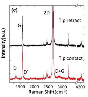
In this work exploring the origin of graphene defects, the TERS tip performed a double function both by artificially inducing the defect and detecting it by enhancing the Raman signal. A MultiView 4000 equipped with nanoparticle-tipped TERS and AFM-TERS feedback induce a reversible defect in the graphene through interaction with the TERS tip; the defect went away when the TERS tip was retracted. The Nanonics instrumentation has several distinct advantages for these kinds of experimental setups:
1. Open optical axis to scanning head, enabling integration with up-right and inverted optical microscopes for TERS measurements on the opaque and transparent samples.
2. Laser-free, tuning fork based feedback resulting in no optical interference between the feedback and Raman signal.
3. Tip and sample scanning in the one scanning head. Tip scanner enables the accurate positioning of the TERS probe relatively to the focused laser for the maximum Raman enhancement.
TERS spectra are shown below of the tip on (red) and off (black) the graphene surface show new bands (D,D+G) induced by the TERS probe. These bands are associated with the creation of the extrinsic deformation on the graphene surface.

Characterization of surface plasmon polariton waveguides
Plasmonics waveguides have unique, attractive features such as 1) allowing co-propagation of optical and electrical signals and 2) tight confinement of the electromagnet mode. A recently published work describes a new configuration of plasmonic waveguides that tries to overcome the device’s well-known obstacle of a limited propagation length, where the loss of light signal occurs due to light absorption in the metal. Authors Uriel Levy and colleagues use a Nanonics Multiview 4000 in this paper [Optics Express, 2014] to characterize the properties of the waveguide and to measure the propagation loss of the waveguide modes. They find comparable propagation loss in their devices, and they suggest significant improvements to the propagation losses with changes to the fabrication process of the device.

Published: Optics Express, Sep 3 2014
Click here for more information on the Nanonics MultiView 4000 system