 Standard AFM technology is currently deficient when it comes to nanoindentation. During indentation, a sample that is in contact with a tip moves up against the tip for the indentation operation. The sample indents a given distance as a result of the force, butthe critical force is unknown, since standard cantilever structures bend. Thus, the distance indented includes both the sample indentation depth and the cantilever bending. Nanonics has solved this problem with its Multiprobe AFM Systems. MultiProbes allow straight diamond or other indenters and frees AFM nanoindentation from cantilever bending constraints.
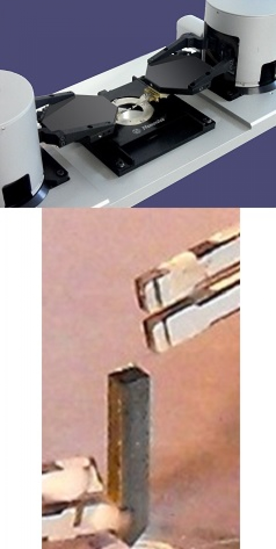
Straight indenters of any type can be bonded to tuning forks, allowing them to be brought in contact with the working surface, while a second AFM probe monitors the indenter’s Z-axis alteration at and only at the straight indenter as the sample is lifted in the Z direction against the indenter. As a result, only the Z-axis alteration of the straight indenter is monitored, independent of any possible tuning fork bending that may occur in spite of the >5000 N/m Force Constant. Up to four probes can be added for on-line monitoring of electrical and thermal parameters during indentation.
For the first time, a state of the art AFM measures true indentation depth versus load, allowing the user to learn:
- Young’s modulus
- Indentation Modulus
- Indentation Creep
- Indentation Creep
- Indentation Hardness
- Progressive Load
- Constant Load
- Multipass Scratch & Wear Tests with Variable Force
- Including Force-displacement curves and scratch and
wear tests with variable force, rate, length and direction - Rate, Length and Direction
- Environmental & temperature control
- High force constant (100 to300 N/m) quartz conical
indenters with customization
- Nanoheater nanoindenters
- NanoIndenters with on-line Raman spectroscopy of
vibrational alterations
Different Indentation Protocols
|
|
|
|
Array of Nanoindentation with various controlled force
|
Nano-Indentation Software module for various NanoIndentation Protocols and with flexible interface for user scripting
|


On-line Load and Unload Curves Versus Distance
|
|
|


The Choice Is Yours From Various Indentation To Scratch Protocols
|
Scanning Probe Microscopy NanoIndentaion array. Bar is 1.7 µm |
A close-up AFM image of NanoIndentaion array. Bar is 750 nm |
AFM image if a nano-scratch performed with Nanonics MultiView Nanoindentation system. bar is 3.0 µm |
|
|
|
|


Variety Of Probes For Hard & Soft Indentation: Shown Indentation of Gold A Soft Material With Nanonics Unique Connical Glass Probes
|
|
|
3D representation of the topographic images before and after Nanoindentation process. Indentation (A) obtained with indenting connical 30 nm glass probe and imaging (B) done on-line with second super-resolution high aspect ratio probe |

Ultrahigh Control Of Load Parameters and Indentation Depth
|
|
|
|
NanoIndentation obtained on SiO2 thin layer in Si obtained with 50nm Berkovich Diamond tip: B) Line profile crossing the nanoindentation areas shows a depth of 36.5nm C) AFM topographic image of a nanoindentation obtained with a load of50µN. D) Line profile crossing the nanoindentation areas shows a depth of 15.08nm |
|


On-line Raman Chemical Analysis
|
On-line AFM/Raman Characteristics of Silicon Indentation a) AFM image of Silicon Indentation b) Indentation Height line profile c) On-line Raman Spectra at marked pints on b showing the different stress level of the indentation patterns |
|
|

